| Part Number |
Description |
Alternative Part Number / Remarks |
| J01031002A |
TRIMS-2 TRBT1.6-W-5-L1 |
TRBT1.6-W-5-L1 |
| J0401006A |
DIODE |
RLS4148 |
| J0402001A |
RECTIFIER DIODE [1N5819] |
1N5819 |
| J0402006A |
DIODE[LL4148] |
LL4148 |
| J0402007A |
DIODE |
SK14 |
| J0403004A |
ZENER DIODE [MMBZ27VCLT1] |
MMBZ27VCLT1 |
| J0403012A |
ZENER DIODE[MMBZ27VDLT/DAN202K] |
MMBZ27VDLT/DAN202K |
| J0403014A |
ZENER DIODE |
MMBZ27VDC |
| J05021001A |
PNP_TRANSISTOR |
2SB1390 |
| J0503001A |
DALINGTON SINK DRIVER[TD62082AF] |
TD62082AF |
| J0601009A |
CHIP LED |
CL-150-HR-CD |
| J0601013A |
LED [CL-200HR] |
CL-200HR |
| J0601027A |
SMD LED[HT-150GQ-DT] |
HT-150GQ-DT |
| J0601038A |
LAMP LED[PL-RA321LWM] |
PL-RA321LWM |
| J0601040A |
LED(DC24V,YEL)[10-5312.3134] |
10-5312.3134 |
| J0601041A |
LED(DC24V,RED)[10-5312.3132] |
10-5312.3132 |
| J0601042A |
LED(DC24V,GRN)[10-5312.3135] |
10-5312.3135 |
| J0601046A |
LED[LST676] |
LST676 |
| J0601047A |
LED[SLR-342VRT] |
SLR-342VRT |
| J0601048A |
LED[LRU3000 (3φ)] |
LRU3000 (3φ) |
| J0601049A |
LED[HT-150GQ-DT (GREEN)] |
HT-150GQ-DT (GREEN) |
| J0601050A |
LED[HT-150HQ-DT (AMBER)] |
HT-150HQ-DT (AMBER) |
| J0601051A |
LED[HT-150YQ-DT (YELLOW)] |
HT-150YQ-DT (YELLOW) |
| J0601052A |
LED[HT-150-HQ] |
HT-150-HQ |
| J0601053A |
LED[LED-4P] |
LED-4P |
| J06011001A |
LED |
SLR-342MG |
| J0604007A |
PHOTO COUPLER[TLP281-4] |
TLP281-4 |
| J0604013A |
PHOTO COUPLER[TLP280-4] |
TLP280-4 |
| J0604015A |
PHOTO COUPLER[TLP280] |
TLP280 |
| J0604016A |
PHOTO COUPLER |
HCPL-0631 |
| J06041001A |
PHOTO_COUPLER_SMD TLP281-1GB |
TLP281-1GB |
| J0801007A |
CMOS LOGIC IC |
SN74HC138D |
| J0801023A |
CMOS LOGIC IC [SN74HC14D] |
SN74HC14D |
| J0803017A |
TTL IC [SN74F245DW] |
SN74F245DW |
| J0803018A |
TTL IC [SN74HC574DW] |
SN74HC574DW |
| J0803021A |
TTL IC [SN74LS04D] |
SN74LS04D |
| J0803026A |
TTL IC [SN74LS245DW] |
SN74LS245DW |
| J0803095A |
IC LOGIC[SN74S38D] |
SN74S38D |
| J08031003A |
LINE_DECODER |
74HC154 |
| J08031004A |
DC-TO-DC-CONVERTER |
MC34063AP1 |
| J08031005A |
TTL 74F14 |
74F14 |
| J08031006A |
TTL 74LS273 |
74LS273 |
| J0803106A |
HEX NVERTER[74HC04A] |
74HC04A |
| J0803107A |
HEX NVERTER[74HC14] |
74HC14 |
| J0803108A |
FLIP-FLOP[74HC273] |
74HC273 |
| J0803110A |
BEFFER[74HC541D] |
74HC541D |
| J0803113A |
AND GATE[74LV08] |
74LV08 |
| J0803114A |
SCHMITT-TRIGGER[74LV14] |
74LV14 |
| J0803115A |
2 INPUT POSITIVE NAND BUFFER[74S38] |
74S38 |
| J0803116A |
DC TO DC CONVERTER[MC34063AP1] |
MC34063AP1 |
| J0803117A |
FLIP-FLOP[SN74HC273D] |
SN74HC273D |
| J0803119A |
SYSTEM FOR[PST572CM-MMP-3A] |
PST572CM-MMP-3A |
| J0803120A |
HEX IVERTER[SN74F04DR] |
SN74F04DR |
| J0803121A |
RESET IC |
PST574CM |
| J0809010A |
NOT GATE IC[74F04] |
74F04 |
| J0903002A |
H8[H8S/2134 (HD64F2134FA20)] |
H8S/2134 (HD64F2134FA20) |
| J1002013A |
A/D CONVERTER |
AD5334BRU |
| J1006011A |
LINE DRIVER[AM26LS31CD] |
AM26LS31CD |
| J1006022A |
LINE DRIVER[DS90C031TM] |
DS90C031TM |
| J1006023A |
LINE DRIVER[DS26C31TM] |
DS26C31TM |
| J1006026A |
LINE RECEIVER[DS26C32ATM] |
DS26C32ATM |
| J1006027A |
LINE RECEIVER[DS90C032TM] |
DS90C032TM |
| J1006028A |
LINE TRANSCEIVER[IDT74FCT164245T] |
IDT74FCT164245T |
| J1006029A |
LINE TRANSCEIVER[SN74HC245D] |
SN74HC245D |
| J1009003A |
CAN CONTROLLER INTERFACE IC [PCA82C250T] |
PCA82C250T |
| J1009011A |
IC:PCI CONTROL[PCI9030] |
PCI9030 |
| J1009013A |
INTERFACE IC[AS82527] |
AS82527 |
| J10091003A |
SERIALIZE_IC DS90CR283 |
DS90CR283 |
| J10091004A |
DESERIALIZE_IC DS90CR284 |
DS90CR284 |
| J1101001A |
PROGRAMMABLE PROM[XC18V01PC20] |
XC18V01PC20 |
| J11011001A |
18V02 18V02 |
18V02 |
| J11031002A |
SERIAL-EEPROM |
93LC56B/P |
| J11061001A |
SRAM |
IDT7132SA-20J |
| J11061002A |
DUAL_PORT_RAM |
IDT7028L15PFY |
| J1200261 |
RELAY SOCKET [PYF08A] |
PYF08A |
| J1201017A |
AMPLIFIER |
LM358M |
| J1201018A |
AMPLIFIER |
LM358BM |
| J1201033 |
HEX SUPPORT [M3*15 (BOLT-NUT)] |
M3*15 (BOLT-NUT) |
| J1201162 |
HEADER, 10P, ANGLE [DF1B-10DP-2.5DS] |
DF1B-10DP-2.5DS |
| J1202240 |
LOGIC (SMD) [74F245] |
74F245 |
| J1203019A |
IC:VOLTAGE REGULATOR[MAX1623EAP] |
MAX1623EAP |
| J1203022A |
SHUNT REGULATOR[TL431CPK] |
TL431CPK |
| J1203023A |
VOLTAGE REGULATOR[KIA78L05F] |
KIA78L05F |
| J1203024A |
VOLTAGE REGULATOR[KIA78L09F] |
KIA78L09F |
| J1203025A |
VOLTAGE REGULATOR[TPS76818QD] |
TPS76818QD |
| J12031001A |
VOLTAGE-REGULATOR |
AME1085DCDT-3 |
| J1300101 |
DRAWER PULL [HD-108] |
HD-108 |
| J1300121 |
ELBOW FITTING [M-5HLH-4] |
M-5HLH-4 |
| J1300134 |
FLAT WASHER [M3] |
M3 |
| J1300135 |
SPRING WASHER [M3] |
M3 |
| J1300141 |
SOCKET HEAD SCREW [M3*10] |
M3*10 |
| J1300167 |
TRUSS SCREW [M3*6 (SUS)] |
M3*6 (SUS) |
| J1300170 |
SOCKET HEAD SCREW [M3*8] |
M3*8 |
| J1300177 |
SPRING WASHER [M4] |
M4 |
| J1300179 |
HEX NUT [M4 (BLACK)] |
M4 (BLACK) |
| J1300182 |
BUTTON HEAD SOCKET SCREW [M4*10] |
M4*10 |
| J1300183 |
SOCKET HEAD SCREW [M4*10] |
M4*10 |
| J1300185 |
SEMUS NABE SCREW [M4*10 ] |
M4*10 |
| J1300186 |
TRUSS SCREW [M4*10] |
M4*10 |
| J1300191 |
SEMUS NABE SCREW [M4*16 ] |
M4*16 |
| J1300193 |
SOCKET HEAD SCREW [M4*20] |
M4*20 |
| J1300205 |
SEMUS NABE SCREW [M4*8 ] |
M4*8 |
| J1300209 |
FLAT WASHER [M5] |
M5 |
| J1300210 |
SPRING WASHER [M5] |
M5 |
| J1300215 |
BUTTON HEAD SOCKET SCREW [M5*10] |
M5*10 |
| J1300217 |
SOCKET HEAD SCREW [M5*10] |
M5*10 |
| J1300220 |
SOCKET HEAD SCREW [M5*12] |
M5*12 |
| J1300227 |
SOCKET HEAD CAP SCREW [M5*8] |
M5*8 |
| J1300238 |
BUTTON HEAD SOCKET SCREW [M6*10 (SUS)] |
M6*10 (SUS) |
| J1300246 |
SOCKET HEAD SCREW [M6*25] |
M6*25 |
| J1300250 |
FLAT WASHER [M8] |
M8 |
| J1300254 |
SOCKET HEAD SCREW [M8*20] |
M8*20 |
| J1300257 |
SOCKET HEAD SCREW [M8*35] |
M8*35 |
| J1300276 |
FITTING [KQ2L06-01/PL6-01] |
KQ2L06-01/PL6-01 |
| J1300284 |
FITTING [KQ2U06-00/PY6M] |
KQ2U06-00/PY6M |
| J1300399 |
BUTTON HEAD SCREW [M3*6 (SUS)] |
M3*6 (SUS) |
| J1300403 |
BUTTON HEAD SOCKET SCREW [M5*10 (SUS)] |
M5*10 (SUS) |
| J1300419 |
C-RING (SHAFT) [DIA15] |
DIA15 |
| J1300434 |
SOCKET HEAD SCREW [M4*15] |
M4*15 |
| J1300435 |
SOCKET HEAD SCREW [M4*25] |
M4*25 |
| J1300436 |
SOCKET HEAD CAP SCREW [M4*30] |
M4*30 |
| J1300489 |
SEMUS NABE SCREW [M3*6 ] |
M3*6 |
| J1300497 |
SHOULDER BOLT [MSB6.5-10] |
MSB6.5-10 |
| J1300502 |
PIN DOWEL [MS5-10] |
MS5-10 |
| J1300517 |
C-RING [10mm (SHAFT)] |
10MM (SHAFT) |
| J1300682 |
SEMUS NABE SCREW[M3*8 ] |
M3*8 |
| J1300683 |
BUTTON HEAD SOCKET SCREW [M4*8 (SUS)] |
M4*8 (SUS) |
| J1300867 |
TRUSS SCREW [M5*10 (SUS)] |
M5*10 (SUS) |
| J1300902 |
SEMUS NABE SCREW [M4*10 ] |
M4*10 |
| J1300920 |
SOCKET HEAD SCREW [M4*6] |
M4*6 |
| J1300921 |
SOCKET HEAD SCREW [M5*18] |
M5*18 |
| J1301009A |
GAL |
GAL16V8A25LJ |
| J1301011A |
EPLD EPM7160SQC160-10 |
EPM7160SQC160-10 |
| J1301013A |
EPLD [EPM7128SQC100-15] |
EPM7128SQC100-15 |
| J1301029A |
GAL[GAL16V8D-25LJ] |
GAL16V8D-25LJ |
| J13011002A |
GAL |
GAL16V8B-10LJ |
| J13011004A |
XCV200E-6-PQ240 XCV200E-6-PQ240C |
XCV200E-6-PQ240C |
| J13011006A |
CPLD M4A5-128/64-10YC |
M4A5-128/64-10YC |
| J1301187 |
ELBOW FITTING [KQ2L12/PL12-04] |
KQ2L12/PL12-04 |
| J1301188 |
FITTING [KQ2L04-M5/PL4-M5M/SQL04-M5] |
KQ2L04-M5/PL4-M5M/SQL04-M5 |
| J1301189 |
ELBOW FITTING [KQ2L06-02/PL6-02] |
KQ2L06-02/PL6-02 |
| J1301213 |
PLUG [PT 3/8] |
PT 3/8 |
| J1301225 |
SPRING WASHER [M4 (SUS)] |
M4 (SUS) |
| J1301324 |
SET SCREW [M3*5] |
M3*5 |
| J1301378 |
SOCKET HEAD SCREW [M2.5*15] |
M2.5*15 |
| J1301487 |
BUTTON HEAD SOCKET SCREW [M4*10 (SUS)] |
M4*10 (SUS) |
| J1500028 |
PROFILE MOUNT [DIA4.0] |
DIA4.0 |
| J1501009A |
PULSE GENERATOR[X7043] |
X7043 |
| J1700011 |
SPANNER [7mm] |
7MM |
| J1700015 |
PRECISION SCREW DRIVER [6PCS] |
6PCS |
| J1700028 |
SPANNER [46MM |
46MM |
| J2001019A |
탄소피막 고정저항기 [RMHS9 102J] |
RMHS9 102J |
| J2001020A |
탄소피막 고정저항기 [RMHS9 103J] |
RMHS9 103J |
| J2001021A |
탄소피막 고정저항기 [RMHS9 472J] |
RMHS9 472J |
| J2001076A |
RESISTOR [CR-1/4W-1K-J-TR] |
CR-1/4W-1K-J-TR |
| J2004060A |
METAL RESISTOR[CR (1/4W, J3.3KΩ)] |
CR (1/4W, J3.3KΩ) |
| J2004061A |
METAL RESISTOR[MR (1/4W,1Mohm)] |
MR (1/4W,1MOHM) |
| J2004063A |
METAL RESISTOR[0.33Ω 1W] |
0.33Ω 1W |
| J2004064A |
RESISTOR[820 OHM, 1/4W] |
820 OHM, 1/4W |
| J2007050A |
CHIP RESISTOR[RC2012J222CS] |
RC2012J222CS |
| J2007090A |
CHIP RESISTOR[RC2012F201CS (200 Ohm)] |
RC2012F201CS (200 OHM) |
| J20071001A |
RES-CE-CHIP-240KOHM-5-2012 |
MCR10EZHJ244 |
| J20071002A |
CHIP_RESISTOR |
MNR14FOABJ121 |
| J20071003A |
CHIP_RESISTOR |
RC2012J000CS |
| J20071004A |
CHIP_RESISTOR |
RC2012J272CS |
| J20071006A |
RECTANGULAR_CHIP_RESISTOR |
RC2012J682CS(6.8K) |
| J20071008A |
RECTANGULAR_CHIP_RESISTOR |
RC3216F333CS(33KΩ) |
| J20071018A |
ARRAY_RESISTOR |
MNR14-EOA-J561(560Ω) |
| J20071019A |
CHIP_RESISTOR |
RC2012F31R6(31.6Ω) |
| J20071020A |
CHIP_RESISTOR |
RC2012F62(62Ω) |
| J20071043A |
RESISTOR MCR10EZHJ000 (0Ω,1/8W) |
MCR10EZHJ000 (0Ω,1/8W) |
| J2007111A |
RECTANGULAR CHIP RESISTOR[MCR10EZHJ101(1 |
MCR10EZHJ101(100) |
| J2007112A |
RECTANGULAR CHIP RESISTOR[MCR10EZHJ242(2 |
MCR10EZHJ242(2.4K) |
| J2007113A |
RECTANGULAR CHIP RESISTOR[MCR10EZHJ332(3 |
MCR10EZHJ332(3.3K) |
| J2007117A |
RECTANGULAR CHIP RESISTOR[MCR10EZHJ100(1 |
MCR10EZHJ100(10) |
| J2007120A |
RECTANGULAR CHIP RESISTOR[MCR10EZHJ111(1 |
MCR10EZHJ111(110K) |
| J2007126A |
RECTANGULAR CHIP RESISTOR[MCR03 EZH F 10 |
MCR03 EZH F 101 (100 Ω) |
| J2007127A |
RECTANGULAR CHIP RESISTOR[MCR03 EZH J 39 |
MCR03 EZH J 390 (39 Ω) |
| J2007128A |
RECTANGULAR CHIP RESISTOR[MCR10 EZH F 47 |
MCR10 EZH F 472 (4.7KΩ, 1/8W) |
| J2007130A |
RECTANGULAR CHIP RESISTOR[MCR10 EZH J 12 |
MCR10 EZH J 121 (120Ω, 1/8W) |
| J2007131A |
RECTANGULAR CHIP RESISTOR[MCR10 EZH J 27 |
MCR10 EZH J 271 (270Ω, 1/8W) |
| J2007132A |
RECTANGULAR CHIP RESISTOR[MCR10 EZH J 56 |
MCR10 EZH J 561 (560Ω, 1/8W) |
| J2007133A |
RECTANGULAR CHIP RESISTOR[MCR10 EZH J 62 |
MCR10 EZH J 622 (6.2KΩ, 1/8W) |
| J2007135A |
RECTANGULAR CHIP RESISTOR[MNR14 E0AB J 4 |
MNR14 E0AB J 472 (4.7 KΩ, 1/8W |
| J2007137A |
RECTANGULAR CHIP RESISTOR[RC2012J122CS(1 |
RC2012J122CS(1.2K) |
| J2007138A |
RECTANGULAR CHIP RESISTOR[RC2012J103CS(1 |
RC2012J103CS(10K) |
| J2007139A |
RECTANGULAR CHIP RESISTOR[RC2012J102CS(1 |
RC2012J102CS(1K) |
| J2007140A |
RECTANGULAR CHIP RESISTOR[RC2012J202CS(2 |
RC2012J202CS(2K) |
| J2007141A |
RECTANGULAR CHIP RESISTOR[RC2012J362CS(3 |
RC2012J362CS(3.6K) |
| J2007143A |
RECTANGULAR CHIP RESISTOR[RC2012J472CS(4 |
RC2012J472CS(4.7K) |
| J2007144A |
RECTANGULAR CHIP RESISTOR[MCR10EZHJ103(1 |
MCR10EZHJ103(10K) |
| J2007145A |
RECTANGULAR CHIP RESISTOR[MCR10EZHJ472(4 |
MCR10EZHJ472(4.7K) |
| J2007146A |
ARRAY RESISTOR[MNR14-EOA-J102(1K)] |
MNR14-EOA-J102(1K) |
| J2007147A |
ARRAY RESISTOR[MNR14-EOA-J103(10K)] |
MNR14-EOA-J103(10K) |
| J2007148A |
ARRAY RESISTOR[MNR14-EOA-J222(2.2K)] |
MNR14-EOA-J222(2.2K) |
| J2007149A |
ARRAY RESISTOR[MNR14-EOA-J333(3.3K)] |
MNR14-EOA-J333(3.3K) |
| J2007150A |
ARRAY RESISTOR[MNR14-EOA-J472(4.7K)] |
MNR14-EOA-J472(4.7K) |
| J2007151A |
RECTANGULAR CHIP RESISTOR[RC2012J100CS(1 |
RC2012J100CS(10) |
| J2007152A |
RECTANGULAR CHIP RESISTOR[RC2012J101CS(1 |
RC2012J101CS(100) |
| J2007153A |
RECTANGULAR CHIP RESISTOR[RC2012J114CS(1 |
RC2012J114CS(110K) |
| J2007154A |
RECTANGULAR CHIP RESISTOR[RC2012J220CS(2 |
RC2012J220CS(22) |
| J2007156A |
RECTANGULAR CHIP RESISTOR[RC2012J242CS(2 |
RC2012J242CS(2.4K) |
| J2007157A |
RECTANGULAR CHIP RESISTOR[RC2012J302CS(3 |
RC2012J302CS(3K) |
| J2007158A |
RECTANGULAR CHIP RESISTOR[RC2012J332CS(3 |
RC2012J332CS(3.3K) |
| J2007160A |
RECTANGULAR CHIP RESISTOR[RC2012J681CS(6 |
RC2012J681CS(680) |
| J2007162A |
RECTANGULAR CHIP RESISTOR |
MCR18EZHF31R6 (31.6Ω, 1/4W) |
| J2007163A |
RECTANGULAR CHIP RESISTOR |
MNR14-EOA-J331(330Ω) |
| J2007164A |
RECTANGULAR CHIP RESISTOR |
RC2012F123CS(12KΩ, 1/8W) |
| J2007165A |
RECTANGULAR CHIP RESISTOR |
RC2012F303CS(30KΩ, 1/8W) |
| J2007166A |
RECTANGULAR CHIP RESISTOR |
RC3216F010CS (1Ω, 1/4W) |
| J2007168A |
RECTANGULAR CHIP RESISTOR |
RC3216F15R4CS(15.4Ω, 1/4W) |
| J2029010A |
REGENERATIVE RESISTOR[IRN150S] |
IRN150S |
| J2100007 |
SQUARE NUT M4 [0131-641702] |
0131-641702 |
| J2100009 |
MANIFOLD [0131-611008] |
0131-611008 |
| J2100018 |
NUT FOOT [0131-611026] |
0131-611026 |
| J2101013A |
ROTARY RESISTOR[GF06P-10K] |
GF06P-10K |
| J21011001A |
VARIABLE_RESISTOR |
GFO6P 10K |
| J2101818 |
IDLER SHAFT-S [0135-641105] |
0135-641105 |
| J2203010A |
CHIP CERAMIC CAPACITOR[CL21B102KBNC] |
CL21B102KBNC |
| J2203012A |
CHIP CAPACITOR[CL21B473KBNC (0.047uF)] |
CL21B473KBNC (0.047UF) |
| J2203013A |
CHIP CAPACITOR[CL21B103KBNC (0.01uF)] |
CL21B103KBNC (0.01UF) |
| J2203014A |
CHIP CAPACITOR[CL21B471KBNC (470pF)] |
CL21B471KBNC (470PF) |
| J2203024A |
CERAMIC CAPACITOR[CS2012Y5V104Z500NRB] |
CS2012Y5V104Z500NRB |
| J2203025A |
CERAMIC CAPACITOR[CS2012X7R103K500NR] |
CS2012X7R103K500NR |
| J2203028A |
CERAMIC CAPACITOR[CS2012X7R104K500NRB] |
CS2012X7R104K500NRB |
| J2203029A |
CERAMIC CAPACITOR[CS2012X7R104K500NRB (1 |
CS2012X7R104K500NRB (100UF/50V |
| J2203030A |
CERAMIC CAPACITOR[CS2012X7R562K500NR] |
CS2012X7R562K500NR |
| J2203031A |
CERAMIC CAPACITOR[CS2012Y5V105Z160NRE (1 |
CS2012Y5V105Z160NRE (1,000UF/1 |
| J2203032A |
CERAMIC CAPACITOR[CL10F104ZBNC] |
CL10F104ZBNC |
| J2203033A |
CERAMIC CAPACITOR[CL21B103KBNC (103)] |
CL21B103KBNC (103) |
| J2203034A |
CERAMIC CAPACITOR[CL21B104KBNC (104)] |
CL21B104KBNC (104) |
| J2203035A |
CERAMIC CAPACITOR[CL21B471KBNC(470PF)] |
CL21B471KBNC(470PF) |
| J2203039A |
CERAMIC CAPACITOR |
CL21B104KBNC (0.1uF/50V) |
| J2203040A |
CERAMIC CAPACITOR |
CL21B471KBNC(470PF/50V) |
| J22031002A |
CERAMIC_CAPACITOR |
CS2012X7R103K500NRB |
| J22031003A |
CERAMIC_CAPACITOR |
CS2012Y5V105Z160NRE (1uF/16V) |
| J22031005A |
CERAMIC_CHIP_CAPACITOR CL21B102KBNC |
CL21B102KBNC |
| J22031006A |
CERAMIC_CAPACITOR |
MCH215F104ZK(0.1UF/50V) |
| J22031025A |
CERAMIC_CAPACITOR CL21B223JBNC (22nF/50V |
CL21B223JBNC (22nF/50V) |
| J2209020A |
CERAMIC CAPACITOR[HC69R2J104K (0.1uF 630 |
HC69R2J104K (0.1UF 630V) |
| J2209021A |
CERAMIC CAPACITOR[KME50VB100 (100uF /50V |
KME50VB100 (100UF /50V) |
| J2401019A |
CAP(전해) |
KME 50VB100(SG 50V 100uF) |
| J2401049A |
ALUMINUM CAPACITOR[220uF/16V] |
220UF/16V |
| J2401050A |
ALUMINUM CAPACITOR[220uF/25V] |
220UF/25V |
| J2401054A |
ELECTROLYTIC CONDENSER[SHL 50V 100uF 85 |
SHL 50V 100UF 85℃ |
| J2401055A |
ALUMINUM CAPACITOR[10UF/25V] |
10UF/25V |
| J2401056A |
ALUMINUM CAPACITOR[330uF/16V] |
330UF/16V |
| J2401057A |
ALUMINUM CAPACITOR[470uF/16V] |
470UF/16V |
| J2401058A |
ALUMINUM CAPACITOR[47uF/50V] |
47UF/50V |
| J2401059A |
ALUMINUM CAPACITOR |
100UF/16V |
| J2401060A |
ALUMINUM CAPACITOR |
100UF/50V |
| J2401061A |
ALUMINUM CAPACITOR |
470UF/16V |
| J24011001A |
ALUMINUM_CAPACITOR |
220UF/35V |
| J2403042A |
TANTALUM CAPACITOR[TCSCS1C106MBAR (10uF/ |
TCSCS1C106MBAR (10UF/16V) |
| J2403043A |
TANTALUM CAPACITOR[TCSCS1C476MDAR (47uF/ |
TCSCS1C476MDAR (47UF/16V) |
| J2403044A |
TANTALUM CAPACITOR[TCSCS1V106MCAR (10uF/ |
TCSCS1V106MCAR (10UF/35V) |
| J2403045A |
TANTALUM CAPACITOR[TCSCS1D105MAAR] |
TCSCS1D105MAAR |
| J2403046A |
TANTALUM CAPACITOR[TCSCS1D106MBAR] |
TCSCS1D106MBAR |
| J24041003A |
ALUMINUM_CAPACITOR |
4.7UF/35V |
| J2501009A |
PLASTIC FILM CAPACITOR[TM 630V 104] |
TM 630V 104 |
| J2501011A |
C-ELEC-DIP |
0.1uF/630V |
| J26051001A |
TRANSFOMER 5KVA, 3PHASE |
5KVA, 3PHASE |
| J2701002A |
INDUCTOR |
DR-4 10mH |
| J2702003A |
BARE PCB[SMT3106-471M] |
SMT3106-471M |
| J2702004A |
COIL[220uH-0.5A] |
220UH-0.5A |
| J2703004A |
SMD INDUCTOR[SMT3106-471M (4.7uH)] |
SMT3106-471M (4.7UH) |
| J2704002A |
INDUCTOR [CIC31J121NC] |
CIC31J121NC |
| J2804020A |
OSCILLATOR[SCO-105-16.384MHz] |
SCO-105-16.384MHZ |
| J2804022A |
OSCILLATOR[SCO-105 (20.000MHz)] |
SCO-105 (20.000MHZ) |
| J28041001A |
OSCILLATOR |
SCO-063S(10MHZ) |
| J28041002A |
OSCILLATOR |
SCO-105 (20.000MHZ) |
| J28041003A |
OCILLATOR SCO-105-40MHZ |
SCO-105-40MHZ |
| J29011001A |
NOISE_FILTER UF20TBH |
UF20TBH |
| J29011002A |
NOISE_FILTER_PC UF5SBS |
UF5SBS |
| J2909003A |
CLAMP FILTER FOR CABLE[ZCAT3035-1330-M-K |
ZCAT3035-1330-M-K |
| J3104018A |
STEPPING MOTOR[2K-M544] |
2K-M544 |
| J31041014A |
STEP_MOTOR 2S56Q-01842SR2 |
2S56Q-01842SR2 |
| J3105010A |
COOLING FAN[4715MS-22T-B50] |
4715MS-22T-B50 |
| J3105022A |
DC FAN(VME용)[EC8015L12B(15mm)] |
EC8015L12B(15MM) |
| J3105024A |
CASE FAN |
EC8025M12B |
| J31051003A |
CPU_COOLER CRUX P5M2 |
CRUX P5M2 |
| J3108063A |
SERVO MOTOR[MSMA082P1A01] |
MSMA082P1A01 |
| J3108064A |
SERVO MOTOR[MSMA102P1C01] |
MSMA102P1C01 |
| J31081004A |
SERVO_MOTOR_PB PBM423DXC24 |
PBM423DXC24 |
| J31081005A |
SERVO_MOTOR_PB PBM565DXC26 |
PBM565DXC26 |
| J31081010A |
SERVO_MOTOR MMMA3ACN2A |
MMMA3ACN2A |
| J31081013A |
SERVO_MOTOR MSMA5AZP2A |
MSMA5AZP2A |
| J3152016A |
MOTOR DRIVER[KR-55ME-2Z-3Z] |
KR-55ME-2Z-3Z |
| J31521002B |
STEP_MOTOR_DRIVER |
LB340-2AXIS |
| J3153054A |
SERVO MOTOR DRIVER(50W)[MADDT1205] |
MADDT1205 |
| J3153056A |
SERVO MOTOR DRIVER(750W)[MCDDT3520] |
MCDDT3520 |
| J3153057A |
SERVO MOTOR DRIVER(1KW)[MDDDT5540] |
MDDDT5540 |
| J3153059A |
SERVO MOTOR DRIVER-PB[PB1D003P101] |
PB1D003P101 |
| J3153060A |
SERVO MOTOR DRIVER-PB[PB1D002P101] |
PB1D002P101 |
| J31531003A |
SERVO MOTOR DRIVER |
MMDDT2C09 |
| J3204002A |
AIR PRESSURE SENSOR [MPX5100AP] |
MPX5100AP |
| J32110015B |
광전스위치 |
E3T-ST11 2M |
| J3211032A |
PHOTOELECTRIC SENSOR [BYD30-DDT] |
BYD30-DDT |
| J3211048A |
PHOTO SENSOR[E3S-LS3N] |
E3S-LS3N |
| J32111008A |
TEACHING_BEAM LS55-05 |
LS55-05 |
| J3212002A |
PHOTO SENSOR |
EE-SX670A |
| J3212004A |
PHOTO SENSOR |
EE-SX672A |
| J3212015A |
PHOTO SENSOR[EE-SY672] |
EE-SY672 |
| J3212022A |
LIMIT SENSOR [EE-SX674] |
EE-SX674 |
| J3212027A |
MICRO PHOTO SENSOR[PM-L24] |
PM-L24 |
| J3212048A |
MICRO PHOTO SENSOR[PM-U24] |
PM-U24 |
| J3212049A |
AREA SENSOR[BWP20-12] |
BWP20-12 |
| J3301002A |
BEADS[ESFB3040042TS] |
ESFB3040042TS |
| J3301003A |
BEADS[HB-1T2012-601JT (600Ω)] |
HB-1T2012-601JT (600Ω) |
| J33011001A |
CHIP_BEAD HB-1T2012-202JT |
HB-1T2012-202JT |
| J3403049A |
SWITCHING ELEMENT[61-8410.12] |
61-8410.12 |
| J3403050A |
ILLUMINATED PUSHBUTTON ACTUATOR[61-1100. |
61-1100.0 |
| J3403051A |
FRONT BEZEL-SET[61-9933.0] |
61-9933.0 |
| J3403052A |
FRONT BEZEL-SET[61-9932.0] |
61-9932.0 |
| J3403064A |
LENS PLASTIC,YELLOW[61-9642.4] |
61-9642.4 |
| J3403065A |
SWITCHING ELEMENT (2A)[61-8420.12] |
61-8420.12 |
| J3403073A |
SWITCHING ELEMENT(2A)[61-8520.12] |
61-8520.12 |
| J3403074A |
SELECT SWITCH(3-POSITION)[61-4810.0] |
61-4810.0 |
| J3403075A |
SWITCH LEVER[61-9028.50] |
61-9028.50 |
| J3403082A |
EMERGENCY SWITCH ASSY[704.075.2(EM)] |
704.075.2(EM) |
| J34031001A |
SW-PUSH |
AB-15AH |
| J3404005A |
TACTILE SWITCH[B3S-1000] |
B3S-1000 |
| J3406005A |
LOAD SWITCH[PI-25] |
PI-25 |
| J3407009A |
SWITCH[KSD-02H] |
KSD-02H |
| J3407010A |
DIP SWITCH[KSD08S] |
KSD08S |
| J3407011A |
DIP SWITCH[KSD04S] |
KSD04S |
| J3407012A |
DIP SWITCH[KUDC16-SE] |
KUDC16-SE |
| J3407013A |
SQUARE TRIMMING |
3266W-1-102LF |
| J3409007A |
LENS [61-9642.7 (CLEAR)] |
61-9642.7 (CLEAR) |
| J3409020A |
EMERGENCY S/W[704.075.2] |
704.075.2 |
| J3409021A |
EM S/W (2B)[704.900.4] |
704.900.4 |
| J3409029A |
KEYLOCK SWITCH[AS6M-2KT2PB] |
AS6M-2KT2PB |
| J3409031A |
POLY SWITCH[SMD100-2] |
SMD100-2 |
| J3409032A |
POLY SWITCH[SMD200] |
SMD200 |
| J34091002A |
SAFETY_DOOR_SWTICH |
D4NS-2BF |
| J3501028A |
RELAY[MY4N-D2 24VDC] |
MY4N-D2 24VDC |
| J3501029A |
RELAY[MY2N-D2 24VDC] |
MY2N-D2 24VDC |
| J3501036A |
RELAY[JW2SN-DC24V] |
JW2SN-DC24V |
| J3501040A |
MAGNETIC CONTACTOR[LC1D096BD, DC24V, 1A1 |
LC1D096BD, DC24V, 1A1B |
| J35011001A |
RELAY |
S1A050000 |
| J3601006A |
FUSE |
250V, 500mA (20mm) |
| J3601008A |
FUSE SMD200(2A) |
SMD200(2A) |
| J3601018A |
FUSE[250V 5A] |
250V 5A |
| J3601019A |
FUSE[250V 10A] |
250V 10A |
| J3601022A |
POLY SWITCH[MINISMDCO50-2] |
MINISMDCO50-2 |
| J36011002A |
POLYSWITCH |
RUEF250-2 |
| J36011008A |
POLY_FUSE RUEF300 |
RUEF300 |
| J3602010A |
FUSE HOLDER[GF-205B(20)] |
GF-205B(20) |
| J3603015A |
CIRCUIT PROTECTOR[C60a-2P-C16(23812)] |
C60A-2P-C16(23812) |
| J3603016A |
CIRCUIT PROTECTOR[C60a-3P-C16(23825)] |
C60A-3P-C16(23825) |
| J36031004A |
MAIN_CIRCUIT_BREAKER GV2ME22 |
GV2ME22 |
| J3701040A |
CONNECTOR[17JE-13090-02(D1)] |
17JE-13090-02(D1) |
| J3701042A |
CONNECTOR[17JE-23090-02(D1)] |
17JE-23090-02(D1) |
| J3701045A |
CONNECTOR[17JE-37H-1C] |
17JE-37H-1C |
| J3701046A |
HOOD[17JE-09H-1C] |
17JE-09H-1C |
| J3701048A |
CONNECTOR[3ROW 44PIN DSUB(MALE)] |
3ROW 44PIN DSUB(MALE) |
| J3701049A |
CONNECTOR[3ROW 62PIN DSUB(MALE)] |
3ROW 62PIN DSUB(MALE) |
| J3701050A |
CONNECTOR[3ROW 15PIN DSUB(FEMALE)] |
3ROW 15PIN DSUB(FEMALE) |
| J3701051A |
HOOD[DSH-C15(M2.6 CHROM)] |
DSH-C15(M2.6 CHROM) |
| J3701052A |
CONNECTOR[DSC-P15(3ROW)] |
DSC-P15(3ROW) |
| J3701053A |
HOOD[17JE-25H-1C] |
17JE-25H-1C |
| J3701054A |
HOOD[17JE-09HL-1C] |
17JE-09HL-1C |
| J37011001A |
CONNECTOR 10326-52A0-008 |
10326-52A0-008 |
| J37011002A |
CONNECTOR 10126-3000VE |
10126-3000VE |
| J37011003A |
CONNECTOR 172161-1 |
172161-1 |
| J37031001A |
CONNECTOR 10250-6212VC |
10250-6212VC |
| J3704008A |
IC SOCKET [110-99-308-41-001] |
110-99-308-41-001 |
| J3704010A |
RELAY SOCKET[PY14-02] |
PY14-02 |
| J3704011A |
RELAY SOCKET[PY08-02] |
PY08-02 |
| J3704012A |
RELAY CLAMP[PYC-P] |
PYC-P |
| J3705004A |
VIDEO CONNECTOR [903-533P-71A] |
903-533P-71A |
| J3706001A |
CONNECTOR [206043-1] |
206043-1 |
| J3706002A |
CONNECTOR [206044-1] |
206044-1 |
| J3706003A |
CABLE CLAMP [206070-1] |
206070-1 |
| J3706009A |
122RECEP T-BOX |
HR10A-7R-6S |
| J3706016A |
CONNECTOR[SNH-10-12S] |
SNH-10-12S |
| J3711045A |
CONNECTOR |
HIF3BB-60PA-2.54DSA |
| J3711061A |
MOTOR DRIVER PW CON. 4PIN[04JFAT-SAXGF] |
04JFAT-SAXGF |
| J3711062A |
MOTOR DRIVER PW CON. 5PIN[05JFAT-SAXGF] |
05JFAT-SAXGF |
| J3711063A |
MOTOR PW CON. 6PIN[06JFAT-SAXGF] |
06JFAT-SAXGF |
| J3711068A |
CONNECTOR(06P)[51021-0600(MOLEX)] |
51021-0600(MOLEX) |
| J3711069A |
CONNECTOR[8822E-060-171] |
8822E-060-171 |
| J3711070A |
CONNECTOR 8822E-030-171 |
8822E-030-171 |
| J37111008A |
CONNECTOR_HEADER DF1B-18DP-2.5DSA |
DF1B-18DP-2.5DSA |
| J37111010A |
CONNECTOR 8822E-040-171 |
8822E-040-171 |
| J37111011A |
HEADER_PIN A1-28PA-2.54DSA |
A1-28PA-2.54DSA |
| J37111012A |
CONNECTOR 43045-1400 |
43045-1400 |
| J37111015A |
CONNECTOR 8830E-020-170S |
8830E-020-170S |
| J3712004A |
CONTACTOR [66332-7 (MALE)] |
66332-7 (MALE) |
| J3712053A |
TERMINAL[50058] |
50058 |
| J3712057A |
TERMINAL[43030-0005] |
43030-0005 |
| J3712058A |
TERMINAL[5556T] |
5556T |
| J3712059A |
TERMINAL[170361-1] |
170361-1 |
| J3712060A |
TERMINAL[5558T] |
5558T |
| J3712061A |
TERMINAL[BVH-21T-P1.1] |
BVH-21T-P1.1 |
| J3712062A |
TERMINAL[170360-1] |
170360-1 |
| J3712063A |
TERMINAL[170362-1] |
170362-1 |
| J3712064A |
TERMINAL[RCDXK-1] |
RCDXK-1 |
| J3712065A |
TERMINAL[170359-1] |
170359-1 |
| J3712066A |
TERMINAL[BXA-001T-P0.6] |
BXA-001T-P0.6 |
| J3712067A |
TERMINAL[DF1B-2428PCF] |
DF1B-2428PCF |
| J3712068A |
TERMINAL[DF1B-2428SCF] |
DF1B-2428SCF |
| J3712070A |
TERMINAL[RMDX6050D28] |
RMDX6050D28 |
| J3712072A |
TERMINAL[43030-0001] |
43030-0001 |
| J3712075A |
FERRULE |
UA-F4014 |
| J3712083A |
FERRULE |
UA-F2X1518 |
| J3712084A |
RING TERMINAL |
0.5SQ/M4 |
| J3712085A |
TERMINAL |
DF1B-2022SCF |
| J3712086A |
TERMINAL |
170366-1 |
| J3712089A |
TERMINAL |
HIF3-2428SCFA |
| J3712090A |
TERMINAL |
HIF3-2630SCFC |
| J3712091A |
RING TERMINAL |
0.5SQ/M3 |
| J3712092A |
FERRULE |
UA-F0508 |
| J37121001A |
TERMINAL |
66360-3 |
| J37121002A |
TERMINAL_AMP 170365-1 |
170365-1 |
| J37121005A |
TERMINAL 43031-0004 |
43031-0004 |
| J37121006A |
TERMINAL YT396J |
YT396J |
| J37121007A |
TERMINAL_5556T2 5556T2 |
5556T2 |
| J3713008A |
CONNECTOR |
DF1B-2S-2.5R |
| J3713025A |
CONNECTOR 43020-0600 |
43020-0600 |
| J3713028A |
CONNECTOR [43025-0400] |
43025-0400 |
| J3713029A |
CONNECTOR [43025-0600] |
43025-0600 |
| J3713031A |
CONNECTOR [43025-1000] |
43025-1000 |
| J3713038A |
CONNECTOR HOUSING [DF1BA-6EP-2.5RC] |
DF1BA-6EP-2.5RC |
| J3713039A |
CONNECTOR HOUSING [DF1BA-12DEP-2.5RC] |
DF1BA-12DEP-2.5RC |
| J3713042A |
CONNECTOR HOUSING [10150-3000VE] |
10150-3000VE |
| J3713056A |
CONNECT[51030-0930] |
51030-0930 |
| J3713057A |
CONNECT[51103-0400] |
51103-0400 |
| J3713058A |
CONNECT[1-1318119-3] |
1-1318119-3 |
| J3713059A |
CONNECTOR[DF1BA-6DEP-2.5RC] |
DF1BA-6DEP-2.5RC |
| J3713061A |
CONNECTOR[555376-1] |
555376-1 |
| J3713064A |
MOTOR DRIVER MOLEX 커넥터 COVER[MOLEX 54 |
MOLEX 54331-0501 |
| J3713065A |
MOTOR DRIVER ENCODER CONNECTOR COVER[MOL |
MOLEX 54181 |
| J3713070A |
CONNECTOR[3ROW 15PIN DSUB(MALE)] |
3ROW 15PIN DSUB(MALE) |
| J3713071A |
CONNECTOR[43025-1200] |
43025-1200 |
| J3713072A |
CONNECTOR[43025-2000] |
43025-2000 |
| J3713076A |
CONNECTOR[5557-02R] |
5557-02R |
| J3713077A |
CONNECTOR[5557-04R] |
5557-04R |
| J3713078A |
CONNECTOR[5557-10R] |
5557-10R |
| J3713079A |
CONNECTOR[5557-14R] |
5557-14R |
| J3713080A |
CONNECTOR[5557-24R] |
5557-24R |
| J3713082A |
CONNECTOR[5559-04P] |
5559-04P |
| J3713083A |
CONNECTOR[5559-24P] |
5559-24P |
| J3713085A |
CONNECTOR[51021-0800] |
51021-0800 |
| J3713086A |
CONNECTOR[DF1B-10DS-2.5RC] |
DF1B-10DS-2.5RC |
| J3713087A |
CONNECTOR[DF1B-12DS-2.5RC] |
DF1B-12DS-2.5RC |
| J3713088A |
CONNECTOR[DF1B-3ES-2.5RC] |
DF1B-3ES-2.5RC |
| J3713089A |
CONNECTOR[DF1B-4DS-2.5RC] |
DF1B-4DS-2.5RC |
| J3713090A |
CONNECTOR[DF1B-4EP-2.5RC] |
DF1B-4EP-2.5RC |
| J3713091A |
CONNECTOR[DF1B-6DS-2.5RC] |
DF1B-6DS-2.5RC |
| J3713092A |
CONNECTOR[DF1B-6EP-2.5RC] |
DF1B-6EP-2.5RC |
| J3713093A |
CONNECTOR[DF1B-6ES-2.5RC] |
DF1B-6ES-2.5RC |
| J3713094A |
CONNECTOR[DF1B-6S-2.5R] |
DF1B-6S-2.5R |
| J3713096A |
CONNECTOR[DF1BA-10DEP-2.5RC] |
DF1BA-10DEP-2.5RC |
| J3713097A |
CONNECTOR[DF1BA-14DEP-2.5RC] |
DF1BA-14DEP-2.5RC |
| J37131014A |
CONNECTOR 43645-0400 |
43645-0400 |
| J37131015A |
CONNECTOR 43020-1200 |
43020-1200 |
| J37131016A |
CONNECTOR 43025-1400 |
43025-1400 |
| J37131019A |
CONNECTOR 172169-1 |
172169-1 |
| J3713101A |
CONNECTOR[SMS9PDH1] |
SMS9PDH1 |
| J37131020A |
CONNECTOR YH396-05V |
YH396-05V |
| J37131021A |
CONNECTOR 8822E-020-171 |
8822E-020-171 |
| J37131025A |
CONNECTOR 43020-1600 |
43020-1600 |
| J3713103A |
CONNECTOR[XAP-06V-1] |
XAP-06V-1 |
| J3713105A |
CONNECTOR[172159-1] |
172159-1 |
| J3713106A |
CONNECTOR[172167-1] |
172167-1 |
| J3713107A |
CONNECTOR[SMS9R1] |
SMS9R1 |
| J3713108A |
CONNECTOR[DF1B-4ES-2.5RC] |
DF1B-4ES-2.5RC |
| J3713110A |
CONNECTOR[43025-1600] |
43025-1600 |
| J3713111A |
CONNECTOR[43025-1800] |
43025-1800 |
| J3713113A |
CONNECTOR[35317-0220] |
35317-0220 |
| J3713114A |
CONNECTOR[35317-0420] |
35317-0420 |
| J3713115A |
CONNECTOR[35317-1020] |
35317-1020 |
| J3713116A |
CONNECTOR[35317-1420] |
35317-1420 |
| J3713118A |
CONNECTOR[172160-1] |
172160-1 |
| J3713119A |
CONNECTOR |
VHR-2N |
| J3713122A |
CONNECTOR |
HIF3BB-60P-2.54C |
| J3713123A |
CONNECTOR |
HIF3B-34D-2.54R |
| J3713124A |
CONNECTOR |
EE-1001 |
| J3713125A |
CONNECTOR |
DF1BA-4EP-2.5RC |
| J3713127A |
CONNECTOR |
DF1BA-3EP-2.5RC |
| J3713131A |
CONNECTOR |
DF1B-4S-2.5R |
| J3713134A |
CONNECTOR |
DF1B-3S-2.5R |
| J3713136A |
CONNECTOR |
DF1B-3EP-2.5RC |
| J3713138A |
CONNECTOR |
DF1B-2ES-2.5RC |
| J3713139A |
CONNECTOR |
DF1B-2EP-2.5RC |
| J3713140A |
CONNECTOR |
DF1B-24DS-2.5RC |
| J3713141A |
CONNECTOR |
DF1B-24DEP-2.5RC |
| J3713142A |
CONNECTOR |
DF1B-14DS-2.5RC |
| J3713147A |
CONNECTOR |
51021-1200 |
| J3713150A |
CONNECTOR |
172233-1 |
| J3713151A |
CONNECTOR |
172165-1 |
| J3713153A |
CONNECTOR |
172157-1 |
| J3714008A |
FERRULE PIN[UA-F0712] |
UA-F0712 |
| J3714010A |
FERRULE PIN[UA-F2512] |
UA-F2512 |
| J3714012A |
FERRULE[UA-F4012] |
UA-F4012 |
| J3714013A |
FERRULE[UA-F1512] |
UA-F1512 |
| J37141001A |
RING_TERMINAL 0.75SQ/M4 |
0.75SQ/M4 |
| J37141002A |
RING_TERMINAL 1.5SQ/M4 |
1.5SQ/M4 |
| J37141003A |
RING_TERMINAL 2.5SQ/M4 |
2.5SQ/M4 |
| J37141004A |
RING_TERMINAL 2.5SQ/M5 |
2.5SQ/M5 |
| J37141005A |
RING_TERMINAL 2.5SQ/M6 |
2.5SQ/M6 |
| J37141006A |
RING_TERMINAL 4.0SQ/M8 |
4.0SQ/M8 |
| J37141007A |
RING_TERMINAL 4.0SQ/M5 |
4.0SQ/M5 |
| J3716042A |
STOPPER[UA-51] |
UA-51 |
| J3716044A |
TEMINAL BLOCK[WDU 2.5] |
WDU 2.5 |
| J3716046A |
END PLATE[WAP2.5-10] |
WAP2.5-10 |
| J3716047A |
CROSS CONNECTION[ZQV2.5] |
ZQV2.5 |
| J3716066A |
MARKING TAG[WS12/5, BLANK] |
WS12/5, BLANK |
| J3716067A |
FUSE TERMINAL BLOCK[ASK 1] |
ASK 1 |
| J3716070A |
PANEL취부대[GV2-AF02] |
GV2-AF02 |
| J3717003A |
PCB CONNECTOR PCN10-96P-2.54DS |
PCN10-96P-2.54DS |
| J3717011A |
PCB CONNECTOR |
DF1B-3P-2.5DSA |
| J3717014A |
PCB CONNECTOR [DF1B-2P-2.5DSA] |
DF1B-2P-2.5DSA |
| J3717017A |
PCB CONNECTOR [DF1B-12DP-2.5DSA] |
DF1B-12DP-2.5DSA |
| J3717032A |
PCB CONNECTOR [DF1B-10DP-2.5DSA] |
DF1B-10DP-2.5DSA |
| J3717034A |
PCB CONNECTOR [DF1B-4DP-2.5DSA] |
DF1B-4DP-2.5DSA |
| J3717035A |
PCB CONNECTOR [DF1B-6DP-2.5DSA] |
DF1B-6DP-2.5DSA |
| J3717062A |
PCB CONNECTOR [DF1B-24DP-2.5DSA] |
DF1B-24DP-2.5DSA |
| J3717073A |
6P CONNECTOR[53261-0690] |
53261-0690 |
| J37171001A |
CONNECTOR |
8830E-080-170L |
| J37171002A |
CONNECTOR |
DF1B-28DP-2.5DS |
| J37171003A |
CONNECTOR |
HIF3FC-34PA-2.54DSA |
| J37171005A |
CONNECTOR |
53261-1290 |
| J37171006A |
MICRO_FIT_20_SMD 43045-2018 |
43045-2018 |
| J37171007A |
LEAF_STYLE_CONNECTOR 52986-5079 |
52986-5079 |
| J37171012A |
CONNECTOR 8830E-040-170L |
8830E-040-170L |
| J3719035A |
PIN[50083-8160] |
50083-8160 |
| J3719036A |
PIN[50351-8100] |
50351-8100 |
| J3719037A |
PIN[1318107-1] |
1318107-1 |
| J3719055A |
MOTOR DRIVER ENCODER CONNECTOR[MOLEX 551 |
MOLEX 55100-0600 |
| J3719056A |
HEADER PIN[A2-8PA-2.54DSA] |
A2-8PA-2.54DSA |
| J3719057A |
HEADER PIN[A2-2PA-2.54DSA] |
A2-2PA-2.54DSA |
| J3719058A |
CONNECTOR[43045-0412] |
43045-0412 |
| J3719059A |
CONNECTOR[43045-0612] |
43045-0612 |
| J3719060A |
CONNECTOR[43045-1012] |
43045-1012 |
| J3719062A |
CONNECTOR[43045-1212] |
43045-1212 |
| J3719063A |
CONNECTOR[43045-1612] |
43045-1612 |
| J3719064A |
CONNECTOR[43045-1812] |
43045-1812 |
| J3719065A |
CONNECTOR[PCN10-96P-2.54DS] |
PCN10-96P-2.54DS |
| J3719066A |
CONNECTOR[7916-15FA] |
7916-15FA |
| J3719067A |
CONNECTOR[7916-15MA] |
7916-15MA |
| J3719068A |
CONNECTOR[7916-44FA] |
7916-44FA |
| J3719069A |
CONNECTOR[S530-029] |
S530-029 |
| J3719070A |
CONNECTOR[8830E-030-170L] |
8830E-030-170L |
| J3719071A |
CONNECTOR[8830E-060-170L] |
8830E-060-170L |
| J3719075A |
HEADER PIN[A1-10PA-2.54DSA] |
A1-10PA-2.54DSA |
| J3719076A |
CONNECTOR[53047-0810] |
53047-0810 |
| J3719077A |
CONNECTOR[7915-15MTBC] |
7915-15MTBC |
| J3719078A |
CONNECTOR[HPC143210 (S530-027)] |
HPC143210 (S530-027) |
| J3719079A |
CONNECTOR KIT[PC2-D24-CL5G] |
PC2-D24-CL5G |
| J3719080A |
USB,PLUG[USB 01-04-PA] |
USB 01-04-PA |
| J3719081A |
USB,SOCKET[USB 01-04-ST] |
USB 01-04-ST |
| J3719082A |
CONNECTOR[43045-0400] |
43045-0400 |
| J3719083A |
CONNECTOR[43045-0600] |
43045-0600 |
| J3719084A |
CONNECTOR[43045-2000] |
43045-2000 |
| J3719087A |
HEADER PIN[HEADER4X2/A1-8PA-2.54DSA] |
HEADER4X2/A1-8PA-2.54DSA |
| J3719088A |
CONNECTOR |
43045-0800 |
| J3719090A |
CONNECTOR |
43045-1200 |
| J3719091A |
CONNECTOR 43045-1600 |
43045-1600 |
| J3719094A |
CONNECTOR |
54306-5019 |
| J3719099A |
CABLE CLAMP |
MS3057-12A |
| J37191013A |
CONNECTOR_HOOD SKER MDR1350 |
SKER MDR1350 |
| J37191014A |
CONNECTOR_HOOD SKER MDR1350L |
SKER MDR1350L |
| J3719102A |
RUBBER BUSHING |
MS3420-21 |
| J37211001A |
PLUG |
MS3106B 20-4S |
| J37211002A |
PLUG |
MS3106B 20-29S |
| J37211004A |
CONNECTOR 8830E-020-170L |
8830E-020-170L |
| J3722004A |
CONNECTOR[R345-08] |
R345-08 |
| J3801009A |
WIRE[KIV 0.75SQ,BLACK] |
KIV 0.75SQ,BLACK |
| J3801012A |
WIRE[KIV 0.3SQ,RED] |
KIV 0.3SQ,RED |
| J3801013A |
WIRE[KIV 0.3SQ,BLACK] |
KIV 0.3SQ,BLACK |
| J38011001A |
CABLE VCT 4C*4.0SQ |
VCT 4C*4.0SQ |
| J38011003A |
CABLE VCTF 2C*1.5SQ |
VCTF 2C*1.5SQ |
| J38011004A |
CABLE UL1007 AWG20 |
UL1007 AWG20 |
| J38011005A |
CABLE UL1007 AWG24 |
UL1007 AWG24 |
| J3802001A |
동축 CABLE [RG-179] |
RG-179 |
| J3802004A |
CABLE[28AWG*20P] |
28AWG*20P |
| J3802007A |
CABLE[UTP-4PR-24AWG] |
UTP-4PR-24AWG |
| J3802008A |
CABLE[AWM 2725 VW-1 USB TY] |
AWM 2725 VW-1 USB TY |
| J3802009A |
CABLE[AWM 2990 VW-1 TY] |
AWM 2990 VW-1 TY |
| J3802010A |
CABLE |
CO-ECX 1.5C*2V+3P*28AWG |
| J38021003A |
CABLE COVV-SB 4C*0.5SQ |
COVV-SB 4C*0.5SQ |
| J38021004A |
CABLE UL20276 10P*28AWG |
UL20276 10P*28AWG |
| J38021005A |
CABLE UL20276 15P*28AWG |
UL20276 15P*28AWG |
| J38021007A |
CABLE UL20276 28AWG*(20P+10C)AMESB |
UL20276 28AWG*(20P+10C)AMESB |
| J3809016A |
COAXIAL CABLE[UL20726 4X30AWG(COAXIAL)] |
UL20726 4X30AWG(COAXIAL) |
| J3811001A |
WIRE[UL1051 AWG28] |
UL1051 AWG28 |
| J3811002A |
WIRE[UL1533 AWG28] |
UL1533 AWG28 |
| J38111001A |
WIRE KIV 1.5SQ, BLACK |
KIV 1.5SQ, BLACK |
| J38111002A |
WIRE KIV 2.5SQ, BLACK |
KIV 2.5SQ, BLACK |
| J38111003A |
WIRE KIV 1.5SQ, GRN/YEL |
KIV 1.5SQ, GRN/YEL |
| J38111004A |
WIRE KIV 2.5SQ, GRN/YEL |
KIV 2.5SQ, GRN/YEL |
| J38111008A |
WIRE KIV 1.0SQ, WHITE |
KIV 1.0SQ, WHITE |
| J3814023A |
HEAT BONDED FLAT CABLE FOR FLEXURE PART[ |
WH FHV-SX(20W) 183C |
| J3814025A |
CABLE[COVV-SB 1P*0.2SQ] |
COVV-SB 1P*0.2SQ |
| J3814026A |
CABLE[COVV-SB 3P*0.2SQ] |
COVV-SB 3P*0.2SQ |
| J3814027A |
CABLE[COVV-SB 6P*0.2SQ] |
COVV-SB 6P*0.2SQ |
| J3814029A |
CABLE[ROVV 10C*0.3SQ] |
ROVV 10C*0.3SQ |
| J3814031A |
CABLE[ROVV 12C*0.3SQ] |
ROVV 12C*0.3SQ |
| J3814032A |
CABLE[ROVV 14C*0.3SQ] |
ROVV 14C*0.3SQ |
| J3814033A |
CABLE[ROVV 15C*0.3SQ] |
ROVV 15C*0.3SQ |
| J3814034A |
CABLE[ROVV 1P*0.5SQ] |
ROVV 1P*0.5SQ |
| J3814035A |
CABLE[ROVV 24C*0.2SQ] |
ROVV 24C*0.2SQ |
| J3814036A |
CABLE[ROVV 2C*0.3SQ] |
ROVV 2C*0.3SQ |
| J3814038A |
CABLE[ROVV 2P*0.3SQ] |
ROVV 2P*0.3SQ |
| J3814040A |
CABLE[ROVV 4C*0.3SQ] |
ROVV 4C*0.3SQ |
| J3814041A |
CABLE[ROVV 4C*0.5SQ] |
ROVV 4C*0.5SQ |
| J3814043A |
CABLE[ROVV 6C*0.2SQ] |
ROVV 6C*0.2SQ |
| J3814045A |
CABLE[UL20012-S 30C*28AWG] |
UL20012-S 30C*28AWG |
| J3814055A |
CABLE[ROVV 2C*0.2SQ] |
ROVV 2C*0.2SQ |
| J3814056A |
CABLE[COVV-SB 24C*0.2SQ] |
COVV-SB 24C*0.2SQ |
| J3814058A |
CABLE |
VCTF 2C*0.75SQ |
| J3814060A |
CABLE |
VCTF 3C*1.25SQ |
| J3814061A |
CABLE |
UL20012-S 40C*28AWG |
| J3814063A |
CABLE UL20276 20PX28AWG |
UL20276 20PX28AWG |
| J3814064A |
CABLE |
ROVV 3C*0.2SQ |
| J3814065A |
CABLE |
COVV-SB 10C*0.2SQ |
| J3814069A |
CABLE |
ROVV-SB 3C*0.2SQ |
| J3814071A |
CABLE |
ROVV 3C*0.3SQ |
| J3814072A |
CABLE |
ROVV 1P*0.3SQ |
| J3814074A |
CABLE |
COVV-SB 2P*0.2SQ |
| J3814075A |
CABLE |
VCTF 4C*0.75SQ |
| J3814079A |
CABLE |
ROVV 30C*0.2SQ |
| J3814080A |
CABLE |
UL20012-S 34CX28AWG |
| J3814081A |
CABLE |
ROVV 60CX0.2SQ |
| J3814083A |
CABLE |
COVV-SB 3PX0.3SQ |
| J3814086A |
CABLE |
ROVV 5C*0.2SQ |
| J38141004A |
CABLE COVV-SB 4P*0.2SQ |
COVV-SB 4P*0.2SQ |
| J38141005A |
CABLE COVV-SB 10P*0.2SQ |
COVV-SB 10P*0.2SQ |
| J38141006A |
CABLE ROVV 2P*0.5SQ |
ROVV 2P*0.5SQ |
| J38141007A |
CABLE ROVV 5P*0.2SQ |
ROVV 5P*0.2SQ |
| J38141011A |
CABLE UL2464 4C*18AWG |
UL2464 4C*18AWG |
| J38141012A |
CABLE UL2464 6P*26AWG |
UL2464 6P*26AWG |
| J38141015A |
CABLE UL20276 40P*28AWG |
UL20276 40P*28AWG |
| J38141019A |
CABLE ROVV 4C*0.2SQ |
ROVV 4C*0.2SQ |
| J3815001A |
EXPAND CABLE[SF-3] |
SF-3 |
| J4103015A |
FIDUCIAL SIDEPCB[FR4,T1.6,FID PCB] |
FR4,T1.6,FID PCB |
| J4104008A |
PCB(CAN CONVEYOR) |
CAN CONVEYOR I/F BOARD VER1.0 |
| J4104012A |
PCB |
SSA-VIS-LIGHT-BOARD |
| J41041002A |
SM411_AXIS_SENSOR_BOARD_BARE_PCB |
VER 1.2 |
| J41041003A |
CONVEYOR_SENSOR_IF_BARE_PCB VER 1.2 |
VER 1.2 |
| J41041005A |
SM411_OUTER_LED_BOARD_BARE_PCB |
VER 1.0 |
| J41041008A |
MEGA_CAMERA_IO_BOARD_PCB VER1.2 |
VER1.2 |
| J4105046A |
BARE PCB[2T, 4LAYER, 200*100 (Ver1.0)] |
2T, 4LAYER, 200*100 (VER1.0) |
| J4105048A |
BARE PCB[200*37*2T,2LY] |
200*37*2T,2LY |
| J4105049A |
BARE PCB[160*110*1.6T,4LY] |
160*110*1.6T,4LY |
| J4105055A |
HEAD ILL VER1.1BARE PCB |
160*130*1.6T,4LY(HEAD ILL) |
| J4105056A |
SM321VISION I/F VER1.2 BARE PCB |
233.35*160*1.6T,4LY(VISION IF) |
| J41051002A |
FEEDER_IO_BARE_PCB |
FEEDER_IO_BARE_PCB |
| J41051003A |
FEEDER_INPUT_EXTENTION_BARE_PCB |
FEEDER INPUT EXTENTION BARE PC |
| J41051005A |
CONVEYOR_SUB_BOARD_BARE_PCB |
CONVEYOR_SUB_BOARD_BARE_PCB |
| J41051006A |
FEEDER_BASE_RIGHT_BOARD_BARE_PCB |
FEEDER_BASE_RIGHT_BOARD_BARE_P |
| J41051007A |
FEEDER_BASE_LEFT_BOARD_BARE_PCB |
FEEDER_BASE_LEFT_BOARD_BARE_PC |
| J41051008A |
FEEDER_BASE_DC_RIGHT_BAREPCB |
FEEDER_BASE_DC_RIGHT_BAREPCB |
| J41051009A |
FEEDER_BASE_DC_LEFT_BAREPCB |
FEEDER_BASE_DC_LEFT_BAREPCB |
| J41051010A |
CP55_PCI_IO |
CP55_PCI_IO |
| J41051014A |
CAN_MASTER_BARE_PCB VER2.0 |
VER2.0 |
| J41051015A |
STEP_CONTROL_BOARD_BARE_PCB VER 1.0 |
VER 1.0 |
| J41051016A |
SM411_VME_IO_BOARD_BARE_PCB |
VER 1.2 |
| J41051017A |
SM411_TWIN_SERVO_BOARD_BARE_PCB |
VER 1.2 |
| J41051018A |
X7043_SEDES_BOARD_BARE_PCB VER 1.4 |
VER 1.4 |
| J41051019A |
X7043_SEDES_SLAVE_BOARD_BARE_PCB VER 1.2 |
VER 1.2 |
| J41051020A |
CONVEYOR_PWR_BOARD_BARE_PCB VER 1.1 |
VER 1.1 |
| J4401036A |
POWER SUPPLY |
TG420-U01(STW) |
| J44011001A |
POWER_SUPPLY UP400S24 |
UP400S24 |
| J44011002A |
DC-DC-CONVERTER PSS6-24-5 |
PSS6-24-5 |
| J4402028A |
PLASTIC FILM CAPACITOR[PP3-24-5] |
PP3-24-5 |
| J47131007B |
TOWER_LAMP |
PRE-P-B-302-RYG(510) |
| J47141001A |
LED-HOLDER |
LED HOLDER(1ROW) |
| J4718007A |
PROBE PIN[SK135RS-AU] |
SK135RS-AU |
| J4718009A |
PROBE PIN[OT397] |
OT397 |
| J4718012A |
PROBE PIN(RECEPTACLE)[SK135SW-AU] |
SK135SW-AU |
| J4718013A |
TEST PIN |
LC-2-G (RED) |
| J48011002A |
SBC HICORE-I9451VLG |
HICORE-I9451VLG |
| J4809051A |
PBPI-8SA[PBPI-8SA] |
PBPI-8SA |
| J4809054A |
VME BACKPLANE |
DSOVME-12J1(REV.C) |
| J48091012A |
MULT_PORT_BOARD 4*COM D I/O |
4*COM D I/O |
| J49011004A |
CPU PENTIUM(D)-945 |
PENTIUM(D)-945 |
| J49011005A |
RAM DDR2-512 |
DDR2-512 |
| J51011005A |
HARD_DISK_DRIVER HDS721680PLA380 |
HDS721680PLA380 |
| J51031005A |
CD_ROM_DRIVE SH-M522C |
SH-M522C |
| J5104001A |
CD-R (RECORDABLE) [MMI BACKUP CD] |
MMI BACKUP CD |
| J51091001A |
USB_MEMORY TS512MJF150 |
TS512MJF150 |
| J5201009A |
MINI USB HUB KEYBOARD |
RKB-371UH-STW-KOR |
| J5202023A |
OPTICAL MOUSE |
M-BJ58 |
| J53011005B |
12INCH_MONITOR |
ST121 |
| J54011003A |
HDD_RACK MOBILE_DOCK(SATA) |
MOBILE_DOCK(SATA) |
| J6001004036 |
SOCKET HEAD CAP SCREW |
M10*40 |
| J6001004038 |
SOCKET HEAD CAP SCREW [M10*40 (BL/ZN)] |
M10*40 (BL/ZN) |
| J6001004536 |
SOCKET HEAD CAP SCREW |
M10*45 |
| J6001200538 |
SOCKET HEAD CAP SCREW [M2*5 (BL/ZN)] |
M2*5 (BL/ZN) |
| J6001200638 |
SOCKET HEAD CAP SCREW [M2*6 (BL/ZN)] |
M2*6 (BL/ZN) |
| J6001200838 |
SOCKET HEAD CAP SCREW [M2*8 (BL/ZN)] |
M2*8 (BL/ZN) |
| J6001201038 |
SOCKET HEAD CAP SCREW [M2*10 (BL/ZN)] |
M2*10 (BL/ZN) |
| J6001250438 |
SOCKET HEAD CAP SCREW [M2.5*4 (BL/ZN)] |
M2.5*4 (BL/ZN) |
| J6001250538 |
SOCKET HEAD CAP SCREW [M2.5*5 (BL/ZN)] |
M2.5*5 (BL/ZN) |
| J6001250638 |
SOCKET HEAD CAP SCREW [M2.5*6 (BL/ZN)] |
M2.5*6 (BL/ZN) |
| J6001250838 |
SOCKET HEAD CAP SCREW [M2.5*8 (BL/ZN)] |
M2.5*8 (BL/ZN) |
| J6001251238 |
SOCKET HEAD CAP SCREW[M2.5*12(Bl/Zn)] |
M2.5*12(BL/ZN) |
| J6001251538 |
SOCKET HEAD CAP SCREW M2.5*15 (BL/Zn) |
M2.5*15 (BL/Zn) |
| J6001300438 |
SOCKET HEAD CAP SCREW [M3*4 (BL/ZN)] |
M3*4 (BL/ZN) |
| J6001300538 |
SOCKET HEAD CAP SCREW [M3*5 (BL/ZN)] |
M3*5 (BL/ZN) |
| J6001300638 |
SOCKET HEAD CAP SCREW [M3*6 (BL/ZN)] |
M3*6 (BL/ZN) |
| J6001300836 |
SOCKET HEAD CAP SCREW |
M3*8 |
| J6001300838 |
SOCKET HEAD CAP SCREW [M3*8 (BL/ZN)] |
M3*8 (BL/ZN) |
| J6001300850 |
SOCKET HEAD CAP SCREW[M3*8 (SUS)] |
M3*8 (SUS) |
| J6001301038 |
SOCKET HEAD CAP SCREW [M3*10 (BL/ZN)] |
M3*10 (BL/ZN) |
| J6001301050 |
SOCKET HEAD CAP SCREW[M3*10 (SUS)] |
M3*10 (SUS) |
| J6001301236 |
SOCKET HEAD CAP SCREW |
M3*12 |
| J6001301238 |
SOCKET HEAD CAP SCREW [M3*12 (BL/ZN)] |
M3*12 (BL/ZN) |
| J6001301538 |
SOCKET HEAD CAP SCREW [M3*15 (BL/ZN)] |
M3*15 (BL/ZN) |
| J6001301838 |
SOCKET HEAD CAP SCREW [M3*18 (BL/ZN)] |
M3*18 (BL/ZN) |
| J6001400638 |
SOCKET HEAD CAP SCREW [M4*6 (BL/ZN)] |
M4*6 (BL/ZN) |
| J6001400650 |
SOCKET HEAD CAP SCREW[M4*6 (SUS)] |
M4*6 (SUS) |
| J6001400836 |
SOCKET HEAD CAP SCREW |
M4*8 |
| J6001400838 |
SOCKET HEAD CAP SCREW [M4*8 (BL/ZN)] |
M4*8 (BL/ZN) |
| J6001401036 |
SOCKET HEAD CAP SCREW |
M4*10 |
| J6001401038 |
SOCKET HEAD CAP SCREW [M4*10 (BL/ZN)] |
M4*10 (BL/ZN) |
| J6001401236 |
SOCKET HEAD CAP SCREW |
M4*12 |
| J6001401238 |
SOCKET HEAD CAP SCREW [M4*12 (BL/ZN)] |
M4*12 (BL/ZN) |
| J6001401538 |
SOCKET HEAD CAP SCREW [M4*15 (BL/ZN)] |
M4*15 (BL/ZN) |
| J6001401636 |
SOCKET HEAD CAP SCREW |
M4*16 |
| J6001401836 |
SOCKET HEAD CAP SCREW M4*18 |
M4*18 |
| J6001402538 |
SOCKET HEAD CAP SCREW M4*25 (BL/Zn) |
M4*25 (BL/ZN) |
| J6001500838 |
SOCKET HEAD CAP SCREW M5*8 (BL/Zn) |
M5*8 (BL/Zn) |
| J6001501036 |
SOCKET HEAD CAP SCREW |
M5*10 |
| J6001501038 |
SOCKET HEAD CAP SCREW [M5*10 (BL/ZN)] |
M5*10 (BL/ZN) |
| J6001501050 |
SOCKET HEAD CAP SCREW[M5*10 (SUS)] |
M5*10 (SUS) |
| J6001501238 |
SOCKET HEAD CAP SCREW [M5*12 (BL/ZN)] |
M5*12 (BL/ZN) |
| J6001501538 |
SOCKET HEAD CAP SCREW [M5*15 (BL/ZN)] |
M5*15 (BL/ZN) |
| J6001501638 |
SOCKET HEAD CAP SCREW M5*16 (BL/Zn) |
M5*16 (BL/Zn) |
| J6001502036 |
SOCKET HEAD CAP SCREW |
M5*20 |
| J6001502038 |
SOCKET HEAD CAP SCREW [M5*20 (BL/ZN)] |
M5*20 (BL/ZN) |
| J6001502050 |
SOCKET HEAD CAP SCREW[M5*20 (SUS)] |
M5*20 (SUS) |
| J6001503036 |
SOCKET HEAD CAP SCREW [M5*30] |
M5*30 |
| J6001503038 |
SOCKET HEAD CAP SCREW [M5*30 (BL/ZN)] |
M5*30 (BL/ZN) |
| J6001601038 |
SOCKET HEAD CAP SCREW [M6*10 (BL/ZN)] |
M6*10 (BL/ZN) |
| J6001601538 |
SOCKET HEAD CAP SCREW [M6*15 (BL/ZN)] |
M6*15 (BL/ZN) |
| J6001602036 |
SOCKET HEAD CAP SCREW |
M6*20 |
| J6001602038 |
SOCKET HEAD CAP SCREW [M6*20 (BL/ZN)] |
M6*20 (BL/ZN) |
| J6001602539 |
SOCKET HEAD CAP SCREW [M6*25] |
M6*25 |
| J6001603538 |
SOCKET HEAD CAP SCREW [M6*35 (BL/ZN)] |
M6*35 (BL/ZN) |
| J6001611050 |
SOCKET HEAD CAP SCREW[M6*110 (SUS)] |
M6*110 (SUS) |
| J6001801038 |
SOCKET HEAD CAP SCREW [M8*10 (BL/ZN)] |
M8*10 (BL/ZN) |
| J6001802038 |
SOCKET HEAD CAP SCREW [M8*20 (BL/ZN)] |
M8*20 (BL/ZN) |
| J6001802536 |
SOCKET HEAD CAP SCREW |
M8*25 |
| J6001802538 |
SOCKET HEAD CAP SCREW [M8*25 (BL/ZN)] |
M8*25 (BL/ZN) |
| J6001802550 |
SOCKET HEAD CAP SCREW[M8*25 (SUS)] |
M8*25 (SUS) |
| J6001804538 |
SOCKET HEAD CAP SCREW [M8*45 (BL/ZN)] |
M8*45 (BL/ZN) |
| J6004002038 |
BUTTON_HEAD_CAP_SCREW M10*20L |
M10*20L |
| J6004501050 |
BUTTON HEAD CAP SCREW |
C-1029-5-10 (M5*10) |
| J6004501550 |
BUTTON HEAD CAP SCREW[C-1209-5-15 (M5*15 |
C-1209-5-15 (M5*15) |
| J6004502050 |
BUTTON HEAD CAP SCREW [C-1029-5-20 (M5* |
C-1029-5-20 (M5*20) |
| J6005300538 |
BUTTON HEAD SOCKET SCREW[M3*5(BL/ZN)세척 |
M3*5(BL/ZN)세척 |
| J6005300638 |
BUTTON HEAD SOCKET SCREW [M3*6 (BL/ZN)] |
M3*6 (BL/ZN) |
| J6005300850 |
BUTTON HEAD SOCKET SCREW |
M3*8 (SUS) |
| J6005400638 |
BUTTON HEAD SOCKET SCREW M4*6 (BL/Zn) |
M4*6 (BL/Zn) |
| J6005401050 |
BUTTON HEAD SOCKET SCREW |
M4*10 (SUS) |
| J6005501050 |
BUTTON HEAD SOCKET SCREW |
M5*10 (SUS) |
| J6005502538 |
BUTTON HEAD SOCKET SCREW[M5*25(BL/Zn)] |
M5*25(BL/ZN) |
| J6006300838 |
FLAT HEAD CAP SCREW [M3*8 (BL/ZN)] |
M3*8 (BL/ZN) |
| J6006400650 |
FLAT HEAD CAP SCREW[M4*6(SUS)] |
M4*6(SUS) |
| J6006401038 |
FLAT HEAD CAP SCREW M4*10 (BL/Zn) |
M4*10 (BL/Zn) |
| J6007300538 |
FLAT HEAD SOCKET SCREW[M3*5,ZN-B] |
M3*5,ZN-B |
| J6007300638 |
FLAT HEAD SOCKET SCREW [M3*6(BL/Zn,세척) |
M3*6 (BL/ZN,세척) |
| J6007300836 |
FLAT HEAD SOCKET SCREW |
M3*8 |
| J6007401538 |
FLAT_HEAD_SOCKET_SCREW |
M4*15 (BL/ZN) |
| J6007801538 |
FLAT HEAD SOCKET SCREW[M8*15 (Bl/Zn)] |
M8*15 (BL/ZN) |
| J6008805504 |
HEX CAP SCREW[M8 X 55L] |
M8 X 55L |
| J6009300637 |
SEMUS NABE SCREW |
M3*6 |
| J6009400837 |
SEMUS NABE SCREW |
M4*8 |
| J6009401037 |
SEMUS NABE SCREW |
M4*10 |
| J6010300338 |
SOCKET SET SCREW [M3*3 (BL/ZN)] |
M3*3 (BL/ZN) |
| J6010300438 |
SOCKET SET SCREW [M3*4 (BL/ZN)] |
M3*4 (BL/ZN) |
| J6010400438 |
SOCKET SET SCREW [M4*4 (BL/ZN)] |
M4*4 (BL/ZN) |
| J6010801050 |
SOCKET SET SCREW [M8*10 (SUS)] |
M8*10 (SUS) |
| J6012300550 |
TRUSS_SCREW |
M3*5 (SUS) |
| J6012400850 |
TRUSS SCREW |
M4*8 (SUS) |
| J6012500850 |
TRUSS_SCREW |
M5*8 (SUS) |
| J6012501050 |
TRUSS SCREW |
M5*10 (SUS) |
| J6015064000 |
SHOULDER SCREW[MSB6-40] |
MSB6-40 |
| J6015601039 |
SHOULDER_SCREW_MSB8-10 |
MSB8-10 |
| J6019002A |
십자홈붙이 둥근머리나사[M3xP0.5xL5] |
M3XP0.5XL5 |
| J6019600610 |
LOW HEAD CAP SCREW[M6-10(4mm wrench)] |
M6-10(4MM WRENCH) |
| J6019600838 |
EXTRA LOW HEAD CAP SCREW[CBSS 6-8] |
CBSS 6-8 |
| J6025300036 |
HEX NUT |
M3 |
| J6025500036 |
HEX NUT |
M5 (BLACK) |
| J6039800038 |
NYLON NUT[M8-풀림방지용] |
M8-풀림방지용 |
| J6041400038 |
CONICAL SPRING WASHER [M4 (BL/ZN)] |
M4 (BL/ZN) |
| J6041500038 |
CONICAL SPRING WASHER M5 (BL/Zn) |
M5 (BL/Zn) |
| J6042000038 |
FLAT WASHER M10 (BL/Zn) |
M10 (BL/Zn) |
| J6042300036 |
FLAT WASHER |
M3 |
| J6042300038 |
FLAT WASHER [M3 (BL/ZN)] |
M3 (BL/ZN) |
| J6042400036 |
FLAT WASHER |
M4 |
| J6042400038 |
FLAT WASHER [M4 (BL/ZN)] |
M4 (BL/ZN) |
| J6042500036 |
FLAT WASHER |
M5 |
| J6042500038 |
FLAT WASHER [M5 (BL/ZN)] |
M5 (BL/ZN) |
| J6042600038 |
FLAT WASHER [M6 (BL/ZN)] |
M6 (BL/ZN) |
| J6042800003 |
WASHER_PWF8 |
PWF8 |
| J6042800036 |
FLAT WASHER [M8] |
M8 |
| J6042800038 |
FLAT WASHER [M8 (BL/ZN)] |
M8 (BL/ZN) |
| J6043000036 |
SPRING WASHER |
M10 |
| J6043300036 |
SPRING WASHER |
M3 |
| J6043300038 |
SPRING WASHER [M3 (BL/ZN)] |
M3 (BL/ZN) |
| J6043400036 |
SPRING WASHER |
M4 |
| J6043400038 |
SPRING WASHER [M4 (BL/ZN)] |
M4 (BL/ZN) |
| J6043500036 |
SPRING WASHER |
M5 |
| J6043500038 |
SPRING WASHER [M5 (BL/ZN)] |
M5 (BL/ZN) |
| J6043600036 |
SPRING WASHER |
M6 |
| J6043600038 |
SPRING WASHER [M6 (BL/ZN)] |
M6 (BL/ZN) |
| J6043800038 |
SPRING WASHER [M8 (BL/ZN)] |
M8 (BL/ZN) |
| J6043800050 |
SPRING WASHER[M8 (SUS)] |
M8 (SUS) |
| J6049000250 |
WASHER WAVY 0.62OD*0.48ID*0.095HGT[SSR-0 |
SSR-0062 |
| J6061004050 |
DOWEL_PIN MS10-40 |
MS10-40 |
| J6061200836 |
DOWEL_PIN MS2-8 |
MS2-8 |
| J6061301000 |
DOWEL PIN [DIA3*10] |
DIA3*10 |
| J6061601000 |
DOWEL PIN [MS6-10] |
MS6-10 |
| J6061603A |
DOWEL PIN[MS4-8] |
MS4-8 |
| J6071150050 |
E-RING[DIA1.5(SUS)] |
DIA1.5(SUS) |
| J6073010136H |
C-RING DIA11(HOLE) |
DIA11(HOLE) |
| J6079000236S |
C-RING(SHAFT) |
DIA22 |
| J6102017A |
PC SLIDE RAIL[3832B-18] |
3832B-18 |
| J6103003A |
HEX SUPPORT |
M3*5 (BOLT-NUT) |
| J6103005A |
HEX SUPPORT |
M3*10 (BOLT-NUT) |
| J6103011A |
HEX SUPPORT |
M3*30 (BOLT-NUT) |
| J6103013A |
HEX SUPPORT[M3*50 (BOLT-NUT)] |
M3*50 (BOLT-NUT) |
| J6103023A |
HEX SUPPORT [M3*20 (BOLT-NUT)] |
M3*20 (BOLT-NUT) |
| J6103029A |
HEX SUPPORTER[M3*10(NUT-NUT, PLASTIC)] |
M3*10(NUT-NUT, PLASTIC) |
| J61031001A |
HEX_SUPPORT |
M3*10(NUT-NUT) |
| J61031003A |
HEX-SUPPORT M3*35 (BOLT-NUT) |
M3*35 (BOLT-NUT) |
| J6107045A |
COIL SPRING[SWU 26-50] |
SWU 26-50 |
| J6107047A |
SPRING[SWU26-70] |
SWU26-70 |
| J61071010A |
TENSION_SPRING AWU6-45 |
AWU6-45 |
| J6108006A |
HINGE PIN[CLBDG8-22] |
CLBDG8-22 |
| J6109006A |
URETAN WHEEL[TP8015-PLY] |
TP8015-PLY |
| J6109007A |
SWIVEL CASTER[TP5040-23-HDP-TLB] |
TP5040-23-HDP-TLB |
| J6109008A |
SWIVEL CASTER[105N] |
105N |
| J6111006A |
PC/VME DUO RACK |
VPC-1208 |
| J6119051A |
HANDLE[AP-2 BLACK] |
AP-2 BLACK |
| J6119056A |
HANDLE BG-10 |
BG-10 |
| J6119066A |
CIRCULAR BUSH[JBHM16-16] |
JBHM16-16 |
| J6119067A |
LOCATION PIN[CFPQA12-16-L19-B3.5] |
CFPQA12-16-L19-B3.5 |
| J6119070A |
BALL PLUNGERS[BSX12] |
BSX12 |
| J63041001A |
O_RING |
3.6X1.5 |
| J63041002A |
O_RING |
J147A05 |
| J6308002A |
URETHANS[AZXS 20-23-M5-7] |
AZXS 20-23-M5-7 |
| J6308003A |
URETHAN CUSHION[AXNSK15-40] |
AXNSK15-40 |
| J6309025A |
FAN보호망[PFC120(FOR 120㎜ FAN)] |
PFC120(FOR 120㎜ FAN) |
| J64021007A |
COVER_PULL P2-42 |
P2-42 |
| J6404001A |
DOOR KEY |
D4DS-K3 |
| J64091005A |
MAGNETIC C-349-2 |
C-179 |
| J6502008A |
LOW PROFILE MOUNTS[DALM5 (NYLON)] |
DALM5 (NYLON) |
| J65041002A |
CABLE_VEYOR HSP0180_2B_28R_21LINK |
HSP0180_2B_28R_21LINK |
| J65041004A |
CABLE_VEYOR HSP0130-1B-18R-28LINK |
HSP0130-1B-18R-28LINK |
| J6601005A |
BALL BEARING |
688ZZ |
| J6601008A |
BALL BEARING |
6000ZZ |
| J6601009A |
BALL BEARING |
6803ZZ |
| J6601020A |
BALL BEARING |
6002ZZ |
| J6601079A |
BALL BEARING [695ZZ] |
695ZZ |
| J6601080A |
BALL BEARING [MR148ZZ] |
MR148ZZ |
| J6601081A |
CAM FOLLOWER [CF3UU-A] |
CF3UU-A |
| J6601088A |
BALL BEARING [605ZZ] |
605ZZ |
| J66011017A |
SUPPORT_UNIT FK12-MP5 |
FK12-MP5 |
| J66011019A |
BEARING 6908ZZ |
6908ZZ |
| J66011020A |
LM_GUIDE SR15W2UU+728LY-II |
SR15W2UU+728LY-II |
| J66011035A |
BALL_BUSH LMU5 |
LMU5 |
| J6601109A |
BALL BEARING[608ZZ] |
608ZZ |
| J6601124A |
SUPPORT UNIT[FK-15] |
FK-15 |
| J6601126A |
BALL BEARING[F608ZZ] |
F608ZZ |
| J6601134A |
BEARING[694ZZ] |
694ZZ |
| J6601140A |
BALL BEARING[684ZZ] |
MR684ZZ |
| J6602076A |
SIMING BELT[384-1.5GT-9] |
384-1.5GT-9 |
| J66021004A |
TIMING_BETL 267-3GT-6 |
267-3GT-6 |
| J66021005A |
BELT_WIDTH_SYNC 025-XL-1457 |
025-XL-1457 |
| J66021006A |
BELT_WORK MAM-5P-1550-6W |
MAM-5P-1550-6W |
| J66021007A |
TIMMING_BELT_WIDTH 180-3GT-9 |
180-3GT-9 |
| J66021008A |
BELT_SHUTTLE_1650 MAM-5P-1169-6W |
MAM-5P-1169-6W |
| J66021009A |
TIMMING_BELT_SW 327-3GT-12 |
327-3GT-12 |
| J66021010A |
TIMMING_BELT_SM 444-3GT-12 |
444-3GT-12 |
| J66021023A |
BELT_SHUTTLE_LONG MAM-5P-1500-6W |
MAM-5P-1500-6W |
| J66021024A |
TIMING_BELT 232-2GT-4 |
232-2GT-4 |
| J66061002A |
Y-BALL_SCREW J66061002A |
J66061002A |
| J66061003A |
X-BALL_SCREW HG1632QS-HEZR-0874*0801-C5F |
HG1632QS-HEZR-0874*0801-C5F |
| J66061004A |
BALL_SCREW 2BTK1405-2.6ZZ+721.5LC7T |
2BTK1405-2.6ZZ+721.5LC7T |
| J66061005A |
CYLINDER AQ2A12-30D |
AQ2A12-30D |
| J6607016A |
LM SLIDE |
BSP 1025 |
| J6607055A |
LM GUIDE [LWLG7C1R140BT1H] |
LWLG7C1R140BT1H |
| J66071013A |
LM_GUIDE-Y SSR25XWY4UUE+1530LYH-2 |
SSR25XWY4UUE+1530LYH-2 |
| J66071014A |
LM_GUIDE-X SSR15XW2UUC1+940LHY-2 |
SSR15XW2UUC1+940LHY-2 |
| J66071015A |
LM_GUIDE SR15W2UU+570LY-II |
SR15W2UU+570LY-II |
| J6611017A |
BALL SPLINE[WSPFL6H200CM/A] |
WSPFL6H200CM/A |
| J66121006A |
COUPLING SFC 040DA2 10B-19B(TYPE B) |
SFC 040DA2 10B-19B(TYPE B) |
| J66121007A |
COUPLING SFC 050DA2 12B-19B(TYPE A) |
SFC 050DA2 12B-19B(TYPE A) |
| J66141001A |
LEAD_SCREW DCM12+566L |
DCM12+566L |
| J6619031A |
SUPPORT UNIT[FK-10] |
FK-10 |
| J6619036A |
LOCK NUT[RN-10] |
RN-10 |
| J6619062A |
CYLINDER JOINT[Y-032B] |
Y-032B |
| J66191007A |
LOCK_NUT RN8 |
RN8 |
| J67010088B |
CYLINDER CM2C32-50-XC3BB |
CM2C32-50-XC3BB |
| J6701018B |
STOPPER CYLINDER 1 [WTS10*30-RS2] |
WTS10*30-RS2 |
| J6701029A |
AIR CYLINDER [BDAS6*5-1A-ZC153A2] |
BDAS6*5-1A-ZC153A2 |
| J6701072C |
AIR CYLINDER[MGPM63A-35-KRIP1567] |
MGPM63A-35-KRIP1567 |
| J67011007B |
CYLINDER |
CQ2B6-2-CJK2341 |
| J67011016B |
AIR_CYLINDER |
TCP1B16-30 |
| J67011017A |
CYLINDER ADR10-30-W13L-R7038 |
ADR10-30-W13L-R7038 |
| J6702021A |
SOLENOID VALVE [K180-4E1-21-DC24V] |
K180-4E1-21-DC24V |
| J6702048A |
SOLENOID VALVE[VA01PEP34-1U-F] |
VA01PEP34-1U-F |
| J6702049A |
SOLENOID VALVE[RCS242-M3-D24NP] |
RCS242-M3-D24NP |
| J67021005A |
SOLENOID_VALVE DV1120-00-R3642-3 |
DV1120-00-R3642-3 |
| J6703007A |
THROTTLE VALVE(ELBOW) |
JNC4-M5 |
| J6703028A |
SPEED CONTROLLER [SS4-M5MA] |
SS4-M5MA |
| J6703031A |
SPEED CONTROLLER[AS1211F-M5-04] |
AS1211F-M5-04 |
| J6703033A |
SPEED CON[AS2201F-01-06S] |
AS2201F-01-06S |
| J6703034A |
SPEED CON[ASP330F-01-06S] |
ASP330F-01-06S |
| J6703037A |
CHECK VALVE[AKH06-00] |
AKH06-00 |
| J67031001A |
CHECK_VALVE AKH04-00 |
AKH04-00 |
| J6705004A |
SILENCER [AN101-01] |
AN101-01 |
| J6705009A |
SILENCER[AS-5] |
AS-5 |
| J67071009A |
VACUUM_GENERATOR VKMH07A-S448S2-B06 |
VKMH07A-S448S2-B06 |
| J67081002A |
ELEMENT_SEPARATOR PFH4000-0005A-6083 |
PFH4000-0005A-6083 |
| J67081003A |
ELEMENT_AIR TAF4000-05-6000 |
TAF4000-05-6000 |
| J67081006A |
MIST_SEPARATOR_ASSY TAC4020-04D-R3643 |
TAC4020-04D-R3643 |
| J67081010A |
ATMOSPHERIC_FILTER LF-M3-Z07-021 |
LF-M3-Z07-021 |
| J6709004A |
REGULATOR [AR1000-M5BG] |
AR1000-M5BG |
| J6709012A |
REGULATOR [TAR4000-04] |
TAR4000-04 |
| J67091007A |
REGULATOR J67091007A |
AR08-T2-D0M0-J267A |
| J67101002A |
DIGITAL_GAGE PS30-103R-N |
PS30-103R-N |
| J6711001A |
ELBOW FITTING |
KQ2L04-M5/PL4-M5M/SQL04-M5 |
| J6711009A |
ELBOW FITTING [KQ2L06-M5] |
KQ2L06-M5 |
| J6711018A |
UNION Y FITTING[KQ2U04-00] |
KQ2U04-00 |
| J6711028A |
ELBOW FITTING [KQ2L04-01] |
KQ2L04-01 |
| J67111015A |
ELBOW_UNION_FEMALE KQ2LF04-M6 |
KQ2LF04-M6 |
| J67111016A |
STRAIGHT_FITTING KQ2H04-M6 |
KQ2H04-M6 |
| J67111017A |
DOUBLE_UNIVERSAL_ELBOW_06 KQ2VD06-02S |
KQ2VD06-02S |
| J67111018A |
DOUBLE_UNIVERSAL_ELBOW_08 KQ2VD08-02S |
KQ2VD08-02S |
| J67111032A |
MIST_FITTING SQV12-04S |
SQV12-04S |
| J6711104A |
STRAIGHT FITTING[KQ2H04-00/PU4] |
KQ2H04-00/PU4 |
| J6711119A |
UNION Y FITTING [KQ2U04-06] |
KQ2U04-06 |
| J6711140A |
STRAIGHT FITTING [SS8-1/8] |
SS8-1/8 |
| J6711147A |
STRAIGHT FITTING KQ2H04-M5 |
KQ2H04-M5 |
| J6711156A |
HOSE NIPPLE [M-5H-4](D/C용) |
M-5H-4 |
| J6711157A |
ELBOW FITTING [KQ2L08-01S] |
KQ2L08-01S |
| J6711180B |
ROTARY JOINT[RC3-M5M-STN] |
RC3-M5M-STN |
| J6711244A |
MALE ELBOW[KQ2L12-03] |
KQ2L12-03 |
| J6711245A |
COUPLING[KD-M5-SA] |
KD-M5-SA |
| J6711247A |
ELBOW FITTING[PT18EF] |
PT18EF |
| J6711256A |
COUPLER[KD-M5-SA34697KR] |
KD-M5-SA34697KR |
| J6711257A |
PLUG[KS-4-M5-SA34698KR] |
KS-4-M5-SA34698KR |
| J6711260A |
ONE TOUCH FITTING[FSE04-M5C] |
FSE04-M5C |
| J6711262A |
MINI FITTING[BC-03-M5] |
BC-03-M5 |
| J6711263A |
MINI FITTING[BE-04-M3] |
BE-04-M3 |
| J6712008A |
PLUG [PT 1/8] |
PT 1/8 |
| J6712013A |
PLUG[PT 1/4 (SUS)](bio) |
PT 1/4 (SUS) |
| J67121004A |
PLUG M3 |
M3 |
| J6713016A |
AIR TUBE (POLYURETHANE) |
U2-4-4*2.5 (BLACK) |
| J6713017A |
AIR TUBE (POLYURETHANE) |
U2-4-6*4 (BLACK) |
| J6713018A |
AIR TUBE (POLYURETHANE) |
U2-4-8*5 (BLACK) |
| J6713020A |
AIR TUBE (POLYURETHANE) |
U2-4-12*8 (BLACK) |
| J6713022B |
COIL TUBE(POLYURETHANE) [J6713022B] |
J6713022B |
| J6713034A |
AIR TUBE(POLYYRETHANE)[U2-4-6*4(YELLOW)] |
U2-4-6*4(YELLOW) |
| J6713035A |
AIR TUBE(POLYYRETHANE)[U2-4-4*2.5(BLUE)] |
U2-4-4*2.5(BLUE) |
| J6713036A |
AIR TUBE(POLYYRETHANE)[U2-4-4*2.5(YELLOW |
U2-4-4*2.5(YELLOW) |
| J6713048A |
MULTI TUBE[UML-408 (BL-BK6-BL)] |
UML-408 (BL-BK6-BL) |
| J67131001A |
TUBE |
J147A03 |
| J67131004A |
AIR_TUBE TU0425C |
TU0425C |
| J6719025A |
GREASE NIPPLE [M6*1.0-STRAIGHT] |
M6*1.0-STRAIGHT |
| J67191001A |
GASKET |
PC2-SG |
| J67191010A |
GAS_SPRING KS2-300-P1-028 |
KS2-300-P1-028 |
| J6739023A |
G1+G2 LENS [BAF10/FD4] |
BAF10/FD4 |
| J6739024A |
G1 LENS (CP45 FID) [BAF10] |
BAF10 |
| J6739025A |
G2 LENS (CP45 FID) [FD4] |
FD4 |
| J6739026A |
G3+G4 LENS (CP60 LSO FID) [FD4/BAF10] |
FD4/BAF10 |
| J6739027A |
G4 LENS (CP60 LSO FID) [FD4] |
FD4 |
| J6739028A |
G3 LENS (CP60 LSO FID) [BAF12] |
BAF12 |
| J6739088A |
LENS PLASTIC,RED[61-9642.2] |
61-9642.2 |
| J6739090A |
LENS PLASTIC,GREEN[61-9642.5] |
61-9642.5 |
| J67391002A |
G1_LENS_SM140165 J67391002A |
J67391002A |
| J67391003A |
G2_LENS_SM140165 J67391003A |
J67391003A |
| J67391004A |
G3_LENS_SM140165 J67391004A |
J67391004A |
| J67391005A |
G4_LENS_SM140165 J67391005A |
J67391005A |
| J6751014A |
CCD CAMERA[VCC-G20E20] |
VCC-G20E20 |
| J6751015A |
CCD CAMERA[SFA-205AL] |
SFA-205AL |
| J67551001A |
FOLDING_MIRROR J67551001A |
J67551001A |
| J6756004A |
SCOTCHCAL FILM[3630-51] |
3630-51 |
| J6756006A |
SCOTCHCAL COLOR FILM[WHITE(3630-20)] |
WHITE(3630-20) |
| J6756008A |
SCOTCHCAL COLOR FILM[SLATE GRAY(3630-61) |
SLATE GRAY(3630-61) |
| J6803001A |
CE MARK (SM)[J6803001A] |
J6803001A |
| J6804002A |
MMI BACKUP DISKETTE LABEL |
DISK LABEL REV1.1 |
| J68041001A |
COMMAND_CODE |
J68041001A |
| J68041002A |
SLOT_BARCODE_R |
J68041002A |
| J68041003A |
SLOT_BARCODE_F |
J68041003A |
| J68060297B |
USERS GUIDE FOR FEEDER |
SM-Type, CHINESE |
| J68061001A |
SM-DOCKINGCART_USERSGUIDE |
SM-Type, CHINESE |
| J68061051A |
SM420-INTRODUCTION-KOR J68061051A |
J68061051A |
| J68061052A |
SM420-HAND_BOOK-KOR J68061052A |
J68061052A |
| J68061053A |
SM420-ADMINISTRATORS_GUIDE-KOR J68061053 |
J68061053A |
| J68061054A |
SM420-MANITENANCE_REFERENCE-KO J68061054 |
J68061054A |
| J68061055A |
SM420-TROUBLESHOOTING_GUIDE-KO J68061055 |
J68061055A |
| J68061056A |
SM420-PROGRAMMING_TUTORIAL-KOR J68061056 |
J68061056A |
| J68061057A |
SM420-TECHNICAL_REFERENCE-KOR J68061057A |
J68061057A |
| J68061058A |
SM420-INTRODUCTION-ENG J68061058A |
J68061058A |
| J68061059A |
SM420-HAND_BOO-ENG J68061059A |
J68061059A |
| J68061060A |
SM420-ADMINISTRATORS_GUIDE-ENG J68061060 |
J68061060A |
| J68061061A |
SM420-MAINTENANCE_REFERENCE-EN J68061061 |
J68061061A |
| J68061062A |
SM420-TROUBLESHOOTING_GUIDE-EN J68061062 |
J68061062A |
| J68061063A |
SM420-PROGRAMMING_TUTORIAL-ENG J68061063 |
J68061063A |
| J68061064A |
SM420-TECHNICAL_REFERENCE-ENG J68061064A |
J68061064A |
| J68061065A |
SM420-INTRODUCTION-CHI J68061065A |
J68061065A |
| J68061066A |
SM420-HAND_BOOK-CHI J68061066A |
J68061066A |
| J68061067A |
SM420-ADMINISTRATORS_GUIDE-CHI J68061067 |
J68061067A |
| J68061068A |
SM420-MAINTENANCE_REFERENCE-CH J68061068 |
J68061068A |
| J68061069A |
SM420-TROUBLESHOOTING_GUIDE-CH J68061069 |
J68061069A |
| J68061070A |
SM420-PROGRAMMING_TUTORIAL-CHI J68061070 |
J68061070A |
| J68061071A |
SM420-TECHNICAL_REFERENCE-CHI J68061071A |
J68061071A |
| J6806247B |
USERS GUIDE FOR FEEDER[SM-Type, KOREAN] |
SM-TYPE, KOREAN |
| J6806255B |
USERS GUIDE FOR FEEDER[SM-Type, ENGLISH] |
SM-TYPE, ENGLISH |
| J6806257B |
SM DOCKING CART USERS GUIDE[KOREAN, SM-T |
KOREAN, SM-TYPE |
| J6806258B |
SM DOCKING CART USERS GUIDE[ENGLISH, SM- |
ENGLISH, SM-TYPE |
| J68080212D |
STICKER-POWER_INPUT_SM320 J68080212D |
J68080212D |
| J68080224B |
STICKER-AIR_INLET J68080224B |
J68080224B |
| J6808023A |
EARTH[0133-612303] |
0133-612303 |
| J68081001C |
STICKER-SERVICE J68081001C |
J68081001C |
| J68081004A |
STICKER-CRUSH_HAND J68081004A |
J68081004A |
| J68081005A |
STICKER-HAZARDOUS_VOLTAGE J68081005A |
J68081005A |
| J68081006A |
STICKER-MAINTENANCE J68081006A |
J68081006A |
| J68081007A |
STICKER-DOOR_KEY J68081007A |
J68081007A |
| J68081008A |
STICKER-EMERGENCY J68081008A |
J68081008A |
| J68081009A |
STICKER-DOOR_OPEN J68081009A |
J68081009A |
| J68081012A |
STICKER-X_AXIS_REAR J68081012A |
J68081012A |
| J68081013A |
STICKER-X_AXIS_FRONT J68081013A |
J68081013A |
| J68081014A |
STICKER-Y_AXIS_FR J68081014A |
J68081014A |
| J68081016A |
STICKER-HIGH_VOLTAGE J68081016A |
J68081016A |
| J68081017A |
STICKER-NO_TOUCH J68081017A |
J68081017A |
| J68081018A |
STICKER-SAFEGUARD J68081018A |
J68081018A |
| J68081020A |
STICKER-SAFEGUARD_KEYHOLDER J68081020A |
J68081020A |
| J68081021A |
STICKER-MAINTENANCE_CE J68081021A |
J68081021A |
| J68081022A |
STICKER-MAINTENANCE_E J68081022A |
J68081022A |
| J68081023A |
STICKER-DOOR_KEY_CE J68081023A |
J68081023A |
| J68081024A |
STICKER-DOOR_KEY_E J68081024A |
J68081024A |
| J68081025A |
STICKER-DOOR_OPEN_CE J68081025A |
J68081025A |
| J68081026A |
STICKER-DOOR_OPEN_E J68081026A |
J68081026A |
| J68081027A |
STICKER-SAFEGUARD_CE J68081027A |
J68081027A |
| J68081028A |
STICKER-SAFEGUARD_E J68081028A |
J68081028A |
| J68081031A |
STICKER-SAFEGUARD_KEYHOLDER_CE J68081031 |
J68081031A |
| J68081032A |
STICKER-SAFEGUARD_KEYHOLDER_E J68081032A |
J68081032A |
| J68081038A |
NAME_STICKER_ROHS J68081038A |
J68081038A |
| J68081039A |
NAME_STICKER_CE J68081039A |
J68081039A |
| J68081040A |
STICKER-EDGE_FIXER J68081040A |
J68081040A |
| J68081043A |
SM411_MODEL_STICKER J68081043A |
J68081043A |
| J68081061A |
NAME_STICKER_CE_ROHS J68081061A |
J68081061A |
| J68081067A |
DIGITAL_GAUGE_STICKER_KOR J68081067A |
J68081067A |
| J68081068A |
DIGITAL_GAUGE_STICKER_ENG J68081068A |
J68081068A |
| J68081069A |
DIGITAL_GAUGE_STICKER_CHI J68081069A |
J68081069A |
| J68081070A |
HANDLE_NUMBER_STICKER J68081070A |
J68081070A |
| J68081071A |
TOP_PLATE_NUMBER_STICKER J68081071A |
J68081071A |
| J68081072A |
COATING_STICKER J68081072A |
J68081072A |
| J69091001A |
SPONGE_TAPE SGNPTA3201000 |
SGNPTA3201000 |
| J7051008C |
BASE-FOOT[J7051008C] |
J7051008C |
| J70510107B |
PCI BRACKET J70510107B |
J70510107B |
| J7051010D |
HOUSING-FOOT[J7051010D] |
J7051010D |
| J70510110C |
BOARD BRACKET |
J70510110C |
| J70510111C |
BOARD COVER |
J70510111C |
| J7051096A |
DRIVER BRACKET-3[J7051096A] |
J7051096A |
| J7051097A |
DRIVER BRACKET-4[J7051097A] |
J7051097A |
| J7051098A |
DRIVER BRACKET-5[J7051098A] |
J7051098A |
| J70511001A |
TWO_STEP_BRACKET J70511001A |
J70511001A |
| J70511003A |
RESISTER_SUPPORT J70511003A |
J70511003A |
| J70511005A |
POWER_SUPPLY_STAND J70511005A |
J70511005A |
| J70511006A |
POWER_SUPPLY_BRACKET J70511006A |
J70511006A |
| J70511007A |
STEP_DRIVER_CASE1 J70511007A |
J70511007A |
| J70511008A |
STEP_DRIVER_CASE2 J70511008A |
J70511008A |
| J70511009A |
TEP_DRIVER_CASE3 J70511009A |
J70511009A |
| J70511010A |
STEP_DRIVER_BRACKET J70511010A |
J70511010A |
| J70511011A |
DRIVER_BRACKET_1 J70511011A |
J70511011A |
| J70511012A |
DRIVER_BRACKET_2 J70511012A |
J70511012A |
| J70511014A |
BOLT_FOOT J70511014A |
J70511014A |
| J70511015D |
BASE_FRAME |
J70511015C |
| J70511018A |
CABLE_DUCT_S-V J70511018A |
J70511018A |
| J70511020A |
STEP_DRIVER_RAIL J70511020A |
J70511020A |
| J70511021A |
RESISTOR_BRACKET J70511021A |
J70511021A |
| J70511023A |
CABLE_DUCT_COVER J70511023A |
J70511023A |
| J70511024A |
CABLE_DUCT_F_L J70511024A |
J70511024A |
| J70511027A |
LOWER_CABLE_DUCT-R J70511027A |
J70511027A |
| J70511028B |
LOWER_CABLE_DUCT-L |
J70511028B |
| J70511029A |
DRIVER_BRACKET-6 J70511029A |
J70511029A |
| J7051105B |
DIN RAIL[J7051105B] |
J7051105B |
| J7051108A |
SPACER FOOT[J7051108A] |
J7051108A |
| J70521003A |
BARCODE-READER-HANGER-BRACKET |
J70521003A |
| J70521020B |
POWER-PANEL-F |
J70521020B |
| J70521022A |
AIR_PANEL_F J70521022A |
J70521022A |
| J70521023A |
MIST_PANEL J70521023A |
J70521023A |
| J70521024A |
SM411_OP_PANEL |
J70521024A |
| J70521025B |
SM330_LOWER_OP_PANEL |
J70521025B |
| J70521026B |
UPPER_COVER_FR |
J70521026B |
| J70521027A |
UPPER_COVER_FL J70521027A |
J70521027A |
| J70521028A |
LOWER_OPEN_COVER_R J70521028A |
J70521028A |
| J70521029A |
LOWER_OPEN_COVER_L J70521029A |
J70521029A |
| J70521030A |
LOWER_OPEN_COVER_RR J70521030A |
J70521030A |
| J70521031A |
INNER_SIDE_COVER_R J70521031A |
J70521031A |
| J70521032A |
INNER_SIDE_COVER_L J70521032A |
J70521032A |
| J70521033B |
COVER_LFM |
J70521033B |
| J70521034B |
LOWER_SIDE_COVER_R |
J70521034B |
| J70521035B |
LOWER_SIDE_COVER_L |
J70521035B |
| J70521036B |
LOWER_SIDE_COVER |
J70521036B |
| J70521037B |
COVER_FRAME |
J70521037B |
| J70521038A |
UPPER_SIDE_COVER J70521038A |
J70521038A |
| J70521039A |
TOP_SIDE_COVER_R J70521039A |
J70521039A |
| J70521040A |
TOP_SIDE_COVER_L J70521040A |
J70521040A |
| J70521041A |
FRAME_PLATE_FR J70521041A |
J70521041A |
| J70521042A |
FRAME_PLATE_FL J70521042A |
J70521042A |
| J70521043A |
FRAME_PLATE_RR J70521043A |
J70521043A |
| J70521044A |
RAME_PLATE_RL J70521044A |
J70521044A |
| J70521045A |
BOTTOM_COVER_FR J70521045A |
J70521045A |
| J70521046A |
BOTTOM_COVER_FL J70521046A |
J70521046A |
| J70521047A |
BOTTOM_COVER_RR J70521047A |
J70521047A |
| J70521048A |
BOTTOM_COVER_RL J70521048A |
J70521048A |
| J70521049B |
SIDE_COVER_SUPPORT |
J70521049B |
| J70521050A |
ACRYL_COVER_HANDLE J70521050A |
J70521050A |
| J70521051B |
CATCH_BRACKET_F |
J70521051B |
| J70521052B |
CATCH_BRACKET_R |
J70521052B |
| J70521053B |
CONVEYOR_COVER |
J70521053B |
| J70521054A |
DOOR_SWITCH_BRACKET J70521054A |
J70521054A |
| J70521058A |
LCD_PLATE J70521058A |
J70521058A |
| J70521059A |
LCD_BRACKET J70521059A |
J70521059A |
| J70521061A |
TOP_COVER_FRAME J70521061A |
J70521061A |
| J70521062A |
TOP_COVER J70521062A |
J70521062A |
| J70521065A |
LOWER_SIDE_HINGE J70521065A |
J70521065A |
| J70521074A |
HINGE_BRACKET J70521074A |
J70521074A |
| J70521075B |
GAS_SPRING_BRACKET1 |
J70521075B |
| J70521076A |
POWER_PANEL_R J70521076A |
J70521076A |
| J70521078A |
JOINT_BLOCK_LH J70521078A |
J70521078A |
| J70521079A |
JOINT_BLOCK_RH J70521079A |
J70521079A |
| J70521080A |
JOINT_BLOCK_MIDDLE J70521080A |
J70521080A |
| J70521081A |
GAS_SPRING_BRACKET2 J70521081A |
J70521081A |
| J70521082A |
GAS_SPRING_BLOCK J70521082A |
J70521082A |
| J70521085A |
DOOR_SWITCH_KEY_BRACKET J70521085A |
J70521085A |
| J70521086B |
LOWER_OPEN_COVER_RL |
J70521086B |
| J70521087A |
WINDOW_HINGE J70521087A |
J70521087A |
| J70521088B |
FB_COVER |
J70521088B |
| J70521089A |
FB_SIDE_COVER_FL J70521089A |
J70521089A |
| J70521090A |
FB_SIDE_COVER_FR J70521090A |
J70521090A |
| J70521091A |
TRAY_CABLE_COVER J70521091A |
J70521091A |
| J70521093A |
MID_JOINT_BLOCK_L J70521093A |
J70521093A |
| J70521094A |
MID_JOINT_BLOCK_R J70521094A |
J70521094A |
| J70521095A |
UPPER_SIDE_COVER_LTS J70521095A |
J70521095A |
| J70521112A |
KEYBOARD_BASE J70521112A |
J70521112A |
| J70521113A |
KEYBOARD_BASE_BRACKET J70521113A |
J70521113A |
| J7052915B |
SCAN BKT[J7052915B] |
J7052915B |
| J7052919A |
CABLE BKT[J7052919A] |
J7052919A |
| J7052921A |
SCANNER COVER BKT[J7052921A] |
J7052921A |
| J7052922B |
KNOB[J7052922B] |
J7052922B |
| J7053047A |
IDLER SPACER-S |
0135-641103 |
| J7053048A |
IDLER SPACER-M |
0135-641104 |
| J70530690B |
SERVO CONNECTOR BKT |
J7053690A |
| J70531011A |
SUPPORT_MOVE_RAIL_TR J70531011A |
J70531011A |
| J70531012B |
SUPPORT_MOVE_RAIL_TL |
J70531012A |
| J70531013A |
SUPPORT_FIX_RAIL_RIGHT J70531013A |
J70531013A |
| J70531014A |
SUPPORT_FIX_RAIL_LEFT J70531014A |
J70531014A |
| J70531015A |
STOPPER_BRACKET_WORK J70531015A |
J70531015A |
| J70531016B |
PCB_GUIDE_RC |
J70531016B01 |
| J70531017B |
PCB_GUIDE_FC |
J70531017B01 |
| J70531019A |
IDLER_SPACER_13 J70531019A |
J70531019A |
| J70531020A |
IDLER_SPACER_11 J70531020A |
J70531020A |
| J70531021A |
IDLER_SHAFT_M J70531021A |
J70531021A |
| J70531022A |
BRACKET_WORK_SENSOR_2 J70531022A |
J70531022A |
| J70531023A |
BRACKET_WORK_SENSOR_1 J70531023A |
J70531023A |
| J70531024A |
BRACKET_TAIL J70531024A |
J70531024A |
| J70531025A |
WIDTH_TENSION_SPACER J70531025A |
J70531025A |
| J70531027A |
TENSION_BRACKET J70531027A |
J70531027A |
| J70531028A |
TENSION_BEARING_PIN J70531028A |
J70531028A |
| J70531029A |
STOPPER_POST J70531029A |
J70531029A |
| J70531030A |
SUPPORT_ST_MOTOR J70531030A |
J70531030A |
| J70531031A |
SM_HOME_SENSOR_DOG J70531031A |
J70531031A |
| J70531032A |
ST_SENSOR_BRACKET_2 J70531032A |
J70531032A |
| J70531033A |
ST_SENSOR_BRACKET_1 J70531033A |
J70531033A |
| J70531035A |
P_WASHER J70531035A |
J70531035A |
| J70531036A |
NUT_HOUSING J70531036A |
J70531036A |
| J70531037A |
MOTOR-BRACKET-SHUTTLE J70531037A |
J70531037A |
| J70531038A |
MOTOR_BRACKET J70531038A |
J70531038A |
| J70531039A |
IDLER_SPACER_45 J70531039A |
J70531039A |
| J70531043A |
BRACKET_SHUTTLE_STP J70531043A |
J70531043A |
| J70531044A |
WD_NUT_BEARING_STOPPER J70531044A |
J70531044A |
| J70531045A |
W_TENSION_TUBE J70531045A |
J70531045A |
| J70531046A |
W_TENSION_SPACER J70531046A |
J70531046A |
| J70531047A |
W_TENSION_SCREW J70531047A |
J70531047A |
| J70531048A |
W_TENSION_PLATE J70531048A |
J70531048A |
| J70531050A |
STOPPER_TOP_PLATE J70531050A |
J70531050A |
| J70531051A |
BACK_UP_PLATE J70531051A |
J70531051A |
| J70531052A |
LOWER_PLATE J70531052A |
J70531052A |
| J70531053A |
UPPER_PLATE J70531053A |
J70531053A |
| J70531054A |
BUT_SENSOR_DOG J70531054A |
J70531054A |
| J70531055A |
SM_R_DOG J70531055A |
J70531055A |
| J70531059A |
DUMP_BOX_SUPPORT J70531059A |
J70531059A |
| J70531060A |
NUT_SPACER J70531060A |
J70531060A |
| J70531062A |
SUPPORT_ST_MOTOR_2 J70531062A |
J70531062A |
| J70531066A |
WORK_WIDTH_SENSOR_DOG J70531066A |
J70531066A |
| J70531071A |
CNT_COVER J70531071A |
J70531071A |
| J70531072A |
CNT_PANEL_FRONT J70531072A |
J70531072A |
| J70531073A |
CNT_PANEL_REAR J70531073A |
J70531073A |
| J70531074A |
WORK_BELT_MOTOR_BRACKET J70531074A |
J70531074A |
| J70531075A |
SHUTTLE_MOTOR_TENSION_PLATE J70531075A |
J70531075A |
| J70531076A |
BRACKET_BD_OUT_SENSOR J70531076A |
J70531076A |
| J70531101A |
COVER_LEFT_PLATE J70531101A |
J70531101A |
| J70531102A |
COVER_RIGHT_PLATE J70531102A |
J70531102A |
| J70531103A |
CV_SUPPORT_M_RAIL J70531103A |
J70531103A |
| J70531104A |
LEFT_PLATE J70531104A |
J70531104A |
| J70531105A |
TOP_COVER_CV J70531105A |
J70531105A |
| J70531107A |
PLATE_LONG_IN J70531107A |
J70531107A |
| J70531108A |
PLATE_LONG_OUT J70531108A |
J70531108A |
| J70531110A |
DUMP_SUPPORT_2 J70531110A |
J70531110A |
| J70531111A |
STOPPER_BRACKET_LONG J70531111A |
J70531111A |
| J70531112A |
STOPPER_POST_LONG J70531112A |
J70531112A |
| J70531113A |
TUBE_SPACER J70531113A |
J70531113A |
| J70531114A |
L_W_SENSOR_BRACKET_1 J70531114A |
J70531114A |
| J70531115A |
L_W_SENSOR_BRACKET_2 J70531115A |
J70531115A |
| J7053184A |
SQUARE NUT M4 |
0131-641702 |
| J7053790A |
LOWER BEARING HOLDER[J7053790A] |
J7053790A |
| J7053791A |
UPPER BEARING HOLDER[J7053791A] |
J7053791A |
| J7053792A |
UPPER LINK PIN[J7053792A] |
J7053792A |
| J7053793A |
LOWER LINK PIN[J7053793A] |
J7053793A |
| J7053794A |
CYLINDER JOINT PIN[J7053794A] |
J7053794A |
| J7053795A |
RING FIXER[J7053795A] |
J7053795A |
| J7053796A |
LOWER LINK SHAFT[J7053796A] |
J7053796A |
| J7053797A |
LOWER LINK END[J7053797A] |
J7053797A |
| J70541004A |
Y_FRAME J70541004A |
J70541004A |
| J70541005A |
Y_MOTOR_BLOCK J70541005A |
J70541005A |
| J70541006A |
BS_REAR_SUPPORT J70541006A |
J70541006A |
| J70541007A |
BRACKET_CABLE_CHAIN-Y J70541007A |
J70541007A |
| J70541008A |
SENSOR_DOG-Y J70541008A |
J70541008A |
| J70541009A |
SENSOR_BKT_HOME-Y J70541009A |
J70541009A |
| J70541010A |
SENSOR_BKT_LIMIT-Y J70541010A |
J70541010A |
| J70541011A |
SENSOR_DOG-CRASH J70541011A |
J70541011A |
| J70541012A |
Y_CABLE_DUCT_SUPPORT J70541012A |
J70541012A |
| J70541015A |
CONNECTOR_PANNEL J70541015A |
J70541015A |
| J70541016A |
3-NIPPLE_BRACKET J70541016A |
J70541016A |
| J70541017A |
2-NIPPLE_BRACKET J70541017A |
J70541017A |
| J70541030A |
BRG_HOUSING_Y J70541030A |
J70541030A |
| J70541031A |
COVER_Y_MOTOR_BLOCK J70541031A |
J70541031A |
| J70541034A |
DRIVER_BOX_BASE J70541034A |
J70541034A |
| J70541035A |
DRIVER_BOX_COVER J70541035A |
J70541035A |
| J70541036A |
DRIVER_BOX_PLATE J70541036A |
J70541036A |
| J70541037A |
SEDES_SLAVE_BOARD_BK J70541037A |
J70541037A |
| J70541038A |
SENSOR_DOG_X J70541038A |
J70541038A |
| J70541099A |
Y_NIPPLE_PLATE J70541099A |
J70541099A |
| J70541100A |
CABLE_SPACER J70541100A |
J70541100A |
| J70541101A |
CONNECTOR_PANEL-Y J70541101A |
J70541101A |
| J70541102A |
FRONT_SENSOR_BKT1 J70541102A |
J70541102A |
| J70541103A |
FRONT_SENSOR_BKT2 J70541103A |
J70541103A |
| J70541104A |
VACUMM_GEN_BKT J70541104A |
J70541104A |
| J70541105A |
GREASE_NIPPLE_NUT J70541105A |
J70541105A |
| J70541108A |
Y_DUCT_BRACKET1 J70541108A |
J70541108A |
| J70541109A |
Y_DUCT_BRACKET2 J70541109A |
J70541109A |
| J7054255A |
CUSHION BRACKET X[J7054255A] |
J7054255A |
| J7054256A |
CUSHION BRACKET Y[J7054256A] |
J7054256A |
| J7054260A |
CABLE FIXER[J7054260A] |
J7054260A |
| J70550431C |
NOZZLE HOLDER |
J70550431C |
| J70550592B |
NOZZLE HOUSING |
J70550592B |
| J70551001A |
BELT_CLAMP1 |
J70551001A |
| J70551002A |
BELT_CLAMP2 |
J70551002A |
| J70551010A |
NOZZLE_PLATE_S |
J70551010A |
| J70551037A |
MIRROR_JOINT J70551037A |
J70551037A |
| J70551038A |
MIRROR_SPRING_BRACKET J70551038A |
J70551038A |
| J70551039A |
INNER_COVER_SUPPORT J70551039A |
J70551039A |
| J70551040A |
SENSOR_BRACKET_R-M J70551040A |
J70551040A |
| J70551041A |
SPRING_POST-FIXED J70551041A |
J70551041A |
| J70551042A |
SPRING_POST-MOVING J70551042A |
J70551042A |
| J70551044A |
AIR_BRACKET_1 J70551044A |
J70551044A |
| J70551045A |
AIR_BRACKET_2 J70551045A |
J70551045A |
| J70551046B |
MIRROR_CAM |
J70551046A |
| J70551047A |
ILLUM_BRACKET J70551047A |
J70551047A |
| J70551059A |
MIRROR_SENSOR_BRACKET J70551059A |
J70551059A |
| J70551098A |
NOZZLE_TIP_CN400 J70551098A |
J70551098A |
| J70551118A |
MIRROR_SHAFT J70551118A |
J70551118A |
| J70551121A |
NOZZLE_CN400 J70551121A |
J70551121A |
| J70551122A |
NOZZLE_PLATE_CN400 J70551122A |
J70551122A |
| J70551126A |
LIGHT_MAPPING_TOOL_FLY_ODD J70551126A |
J70551126A |
| J70551131A |
Z-STOPPER_BOLT J70551131A |
J70551131A |
| J7055140A |
STEEL BALL [DIA2, SUS304] |
DIA2, SUS304 |
| J7055153A |
MIRROR SCREW [J7055153A] |
J7055153A |
| J7055163A |
BEARING HOUSING [J7055163A] |
J7055163A |
| J7055204A |
ARM JOINT [J7055204A] |
J7055204A |
| J7055404B |
NOZZLE HOUSING[J7055404B] |
J7055404B |
| J7055405A |
GUIDE PIN[J7055405A] |
J7055405A |
| J7055408C |
NOZZLE CN040[J7055408C] |
J7055408C |
| J7055409C |
NOZZLE TIP CN040[J7055409C] |
J7055409C |
| J7055412C |
NOZZLE CN065[J7055412C] |
J7055412C |
| J7055413C |
NOZZLE TIP CN065[J7055413C] |
J7055413C |
| J7055424A |
GUIDE PIN-ODD[J7055424A] |
J7055424A |
| J7055477A |
SPRING COMP[J7055477A] |
J7055477A |
| J7055542C |
BALL SPLINE[J7055542C] |
J7055542C |
| J7055543A |
SPLINE HOUSING[J7055543A] |
J7055543A |
| J7055544A |
BEARING COLLAR[J7055544A] |
J7055544A |
| J7055545B |
SPLINE ALIGNER[J7055545B] |
J7055545B |
| J7055548A |
SPRING[J7055548A] |
J7055548A |
| J7055552A |
SENSOR BRACKET R-H[J7055552A] |
J7055552A |
| J7055554A |
SPACER[J7055554A] |
J7055554A |
| J7055555A |
BEARING NUT[J7055555A] |
J7055555A |
| J7055557A |
BEARING HOUSING[J7055557A] |
J7055557A |
| J7055569A |
NOZZLE TIP CN140[J7055569A] |
J7055569A |
| J7055570A |
NOZZLE CN140[J7055570A] |
J7055570A |
| J7055588A |
SPRING[J7055588A] |
J7055588A |
| J7055610A |
NOZZLE HOUSING-ODD[J7055610A] |
J7055610A |
| J7055615A |
NOZZLE HOUSING[J7055615A] |
J7055615A |
| J7055616A |
SPRING[J7055616A] |
J7055616A |
| J7055651A |
NOZZLE CN220(CERAMIC)[J7055651A] |
J7055651A |
| J7055652A |
NOZZLE TIP CN220(CERAMIC)[J7055652A] |
J7055652A |
| J7055655A |
THETA MOTOR PLATE[J7055655A] |
J7055655A |
| J7055656A |
Z-TENSION BRACKET[J7055656A] |
J7055656A |
| J7055658A |
PULLEY PIN[J7055658A] |
J7055658A |
| J7055659A |
BEARING PLATE[J7055659A] |
J7055659A |
| J7055662A |
VACUUM SENSOR BRACKET[J7055662A] |
J7055662A |
| J70561001A |
CYLINDER_BRACKET J70561001A |
J70561001A |
| J70570211E |
BODY-FEEDER BASE |
J70570211E |
| J70570212D |
VERTICAL LOCATOR |
J70570212D |
| J70570234E |
BODY-DC FEEDER BASE |
J70570234E |
| J70570235D |
DC VERTICAL-LOCATOR |
J70570235D |
| J70571006A |
DOCKING_SOL_BRACKET J70571006A |
J70571006A |
| J7057213A |
SIDE CABLE COVER-FB[J7057213A] |
J7057213A |
| J7057214B |
LOWER FRAME[J7057214B] |
J7057214B |
| J7057215C |
SIDE FRAME-R[J7057215C] |
J7057215C |
| J7057216C |
SIDE FRAME-L[J7057216C] |
J7057216C |
| J7057217B |
CROSS-FRAME[J7057217B] |
J7057217B |
| J7057219C |
BOARD COVER[J7057219C] |
J7057219C |
| J7057220C |
WHEEL PLATE[J7057220C] |
J7057220C |
| J7057221B |
SUPPORT ARM-R[J7057221B] |
J7057221B |
| J7057222B |
SUPPORT ARM-L[J7057222B] |
J7057222B |
| J7057223B |
ADJUST BLOCK[J7057223B] |
J7057223B |
| J7057224B |
ADJUST SCREW[J7057224B] |
J7057224B |
| J7057225A |
ADJUST NUT[J7057225A] |
J7057225A |
| J7057226A |
ADJUST WHEEL[J7057226A] |
J7057226A |
| J7057227B |
Z-STOPPER[J7057227B] |
J7057227B |
| J7057229A |
CABLE CLIP[J7057229A] |
J7057229A |
| J7057236A |
SLOT BUSH[J7057236A] |
J7057236A |
| J7057237C |
ANTI-PITCH ARM[J7057237C] |
J7057237C |
| J7057238B |
ANTI-PITCH PIN[J7057238B] |
J7057238B |
| J7057239B |
CABLE HOLDER[J7057239B] |
J7057239B |
| J7057240C |
DOCKING BLOCK-RU[J7057240C] |
J7057240C |
| J7057241B |
DOCKING BLOCK-RL[J7057241B] |
J7057241B |
| J7057242C |
DOCKING BLOCK-LU[J7057242C] |
J7057242C |
| J7057243B |
DOCKING BLOCK-LL[J7057243B] |
J7057243B |
| J7057244B |
SENSOR BRACKET[J7057244B] |
J7057244B |
| J7057246B |
COUPLER HOLDER MOUNT[J7057246B] |
J7057246B |
| J7057247A |
POSITIONNING GUIDE[J7057247A] |
J7057247A |
| J7057250A |
BALL RAIL[J7057250A] |
J7057250A |
| J7057251A |
PIN CABLE RETAINER[J7057251A] |
J7057251A |
| J7057252A |
CART GRIP[J7057252A] |
J7057252A |
| J7057253A |
SIDE COVER[J7057253A] |
J7057253A |
| J7057254C |
BOARD PLANE[J7057254C] |
J7057254C |
| J7057255A |
SIDE CABLE COVER-R[J7057255A] |
J7057255A |
| J7057256A |
SIDE CABLE COVER-L[J7057256A] |
J7057256A |
| J7057257B |
ROLLER COVER-R[J7057257B] |
J7057257B |
| J7057258B |
ROLLER COVER-L[J7057258B] |
J7057258B |
| J7057259A |
ROLLER COVER POST[J7057259A] |
J7057259A |
| J7057260B |
TOP PLATE[J7057260B] |
J7057260B |
| J7057261B |
TOP PLATE-DC[J7057261B] |
J7057261B |
| J7057262B |
CAP-TOP PLATE[J7057262B] |
J7057262B |
| J70600078B |
KVMS BOARD BRACKET [J70600078B] |
J70600078B |
| J70601002A |
RACK_DUCT RACK_DUCT |
RACK_DUCT |
| J7065934A |
BRACKET CABLE[J7065934A] |
J7065934A |
| J7066025A |
COUPLER BKT2[SM1-MF08-091] |
SM1-MF08-091 |
| J7070218C |
SENSOR BRACKET 2[J7070218C] |
J7070218C |
| J7070245A |
LOWER DOOR BRACKET[J7070245A] |
J7070245A |
| J7070297A |
MONITOR CABLE COVER[J7070297A] |
J7070297A |
| J7070322A |
SCANNER COVER[J7070322A] |
J7070322A |
| J7070341A |
WASHER-M4[J7070341A] |
J7070341A |
| J7070352A |
CONNECTOR BRACKET[J7070352A] |
J7070352A |
| J7070353A |
BARCODE COVER[J7070353A] |
J7070353A |
| J7152020A |
WASHER |
0133-612302 |
| J7152027A |
GROUND TERMINAL [J7152027A] |
J7152027A |
| J7152028C |
GROUND BASE(2)[J7152028C] |
J7152028C |
| J71521001A |
MONITOR_HINGE_BLOCK J71521001A |
J71521001A |
| J71521003A |
PROFILE_FRT J71521003A |
J71521003A |
| J71521004A |
PROFILE_REAR J71521004A |
J71521004A |
| J71521006A |
SIDE_PROFILE J71521006A |
J71521006A |
| J71521007A |
PROFILE_RH J71521007A |
J71521007A |
| J71521008A |
JOINT_LR1 J71521008A |
J71521008A |
| J71521010A |
PLATE_WASHER_GUIDE J71521010A |
J71521010A |
| J71521011A |
JOINT_LR2 J71521011A |
J71521011A |
| J71521012A |
PROFILE_LH J71521012A |
J71521012A |
| J7153010B |
ADJUST SHAFT [J7153010B] |
J7153010B |
| J7153033A |
BUSH SPACER |
0135-641110 |
| J7153034A |
CLAMP SHAFT |
0135-641111 |
| J7153036A |
SLIDE GUIDE |
0135-641125 |
| J71531004B |
WORK_REAR_FRAME |
J71531004A |
| J71531005A |
SUPPORT_BRACKET_S J71531005A |
J71531005A |
| J71531006A |
SUPPORT_BRACKET_L J71531006A |
J71531006A |
| J71531007A |
PULLEY_WIDTH_MOTOR J71531007A |
J71531007A |
| J71531008A |
PULLEY_W_MOTOR J71531008A |
J71531008A |
| J71531009A |
PULLEY_B_M J71531009A |
J71531009A |
| J71531010A |
LM_BASE J71531010A |
J71531010A |
| J71531013B |
WORK_FRONT_FRAME |
J71531013A |
| J71531014A |
BASE_SHUTTLE J71531014A |
J71531014A |
| J71531015A |
SUPPORT_UNIT_ST_TAIL J71531015A |
J71531015A |
| J71531016A |
PULLEY_SHUTTLE_WIDTH J71531016A |
J71531016A |
| J71531017A |
PULLEY_S_W_NUT J71531017A |
J71531017A |
| J71531018A |
ENTRY_PCB_GUIDE_1650 J71531018A |
J71531018A |
| J71531019A |
ENTRY_FRAME_01_1650 J71531019A |
J71531019A |
| J71531020A |
ENTRY_FRAME_00_1650 J71531020A |
J71531020A |
| J71531021A |
BLOCK_SHUTTLE_REAR_LEFT J71531021A |
J71531021A |
| J71531022A |
BLOCK_SHUTTLE_FRONT J71531022A |
J71531022A |
| J71531023A |
BLOCK_SHUTTLE_REAR_RIGHT J71531023A |
J71531023A |
| J71531024A |
WIDTH_PULLEY J71531024A |
J71531024A |
| J71531025A |
PULLEY_SHUTTLE_MOTOR J71531025A |
J71531025A |
| J71531041A |
ENTRY_PCB_GUIDE_LONG_F J71531041A |
J71531041A |
| J71531042A |
ENTRY_PCB_GUIDE_LONG_R J71531042A |
J71531042A |
| J71531043A |
LONG_EXTEND_FRONT J71531043A |
J71531043A |
| J71531044A |
LONG_EXTEND_REAR J71531044A |
J71531044A |
| J71531045B |
CLAMP_FRONT_FRAME |
J71531045A |
| J71531046B |
CLAMP_REAR_FRAME |
J71531046A |
| J7153373A |
FIDUCIAL DISK[J7153373A] |
J7153373A |
| J7153418A |
UPPER FREE LINK[J7153418A] |
J7153418A |
| J7153419A |
UPPER DRIVING LINK[J7153419A] |
J7153419A |
| J71541005C |
X_FRAME |
J71541005A |
| J71541007B |
Y1_PLATE |
J71541007A |
| J71541008B |
Y2_PLATE |
J71541008A |
| J71541009A |
BRG_SUPPORT-X J71541009A |
J71541009A |
| J71541010A |
BRG_HOUSING-X J71541010A |
J71541010A |
| J71541015B |
GUIDE_CABLE_CHAIN-X |
J71541015A |
| J71541016A |
HARNESS_SUPPORT J71541016A |
J71541016A |
| J71541017A |
HARNESS_PLATE J71541017A |
J71541017A |
| J71541018A |
CABLEVEYOR_BRACKET J71541018A |
J71541018A |
| J71541019A |
HEAD_BOARD_BRACKET J71541019A |
J71541019A |
| J71541020A |
HEAD_BASE J71541020A |
J71541020A |
| J71541077A |
HEAD_COVER_BRACKET J71541077A |
J71541077A |
| J71541078A |
HEAD_FRONT_COVER J71541078A |
J71541078A |
| J71541079A |
HEAD_TOP_COVER J71541079A |
J71541079A |
| J71550253C |
FRONT BARREL |
A5052-H32.흑색 |
| J71550508C |
SLIDE BODY |
J71550508C |
| J71550511B |
STOPPER J7155511A |
J7155511A |
| J71550513C |
SENSOR DOG-R J71550513C |
J71550513C |
| J71551009B |
MAIN_BODY |
J71551009B |
| J71551010B |
FIDUCIAL_CAMERA_BRACKET |
J71551010B |
| J71551011A |
MIRROR_FRAME J71551011A |
J71551011A |
| J71551013A |
MIRROR_ARM-CAMERA J71551013A |
J71551013A |
| J71551014A |
MIRROR_ARM-PULLEY J71551014A |
J71551014A |
| J71551015A |
INNER_LIGHT_COVER J71551015A |
J71551015A |
| J71551016A |
CAMERA_BOARD_COVER J71551016A |
J71551016A |
| J71551017A |
MIRROR_MOTOR_BRACKET J71551017A |
J71551017A |
| J71551018A |
FIDUCIAL_BLOCK J71551018A |
J71551018A |
| J71551019A |
SIDE_ILLUM_BODY J71551019A |
J71551019A |
| J71551020A |
TIE_MOUNT_1 J71551020A |
J71551020A |
| J71551021A |
TIE_MOUNT_2 J71551021A |
J71551021A |
| J71551022A |
OUTER_ILLUM_BODY J71551022A |
J71551022A |
| J71551025A |
PULLEY-R_AXIS2 J71551025A |
J71551025A |
| J71551026A |
PULLEY-S_AXIS1 J71551026A |
J71551026A |
| J71551043A |
MIRROR_SENSOR_DOG J71551043A |
J71551043A |
| J71551109A |
LOWER_LIGHT_COVER J71551109A |
J71551109A |
| J71551117A |
MANIFOLD J71551117A |
J71551117A |
| J71551125A |
CAMERA_HOLDER J71551125A |
J71551125A |
| J7155197A |
MIRROR 고정판 [J7155197A] |
J7155197A |
| J7155254C |
REAR BARREL[J7155254C] |
J7155254C |
| J7155255A |
FRONT RETAINER [A5052-H32,흑색] |
A5052-H32,흑색 |
| J7155256A |
REAR RETAINER(CP60 LSO FID)[A6063-T6,흑 |
A6063-T6,흑색 |
| J7155509A |
SPLINE ALIGNER CAP[J7155509A] |
J7155509A |
| J7155510A |
JONT[J7155510A] |
J7155510A |
| J7155512A |
SENSOR DOG[J7155512A] |
J7155512A |
| J7155518A |
PULLEY (Z-AXIS 1)[J7155518A] |
J7155518A |
| J7155520A |
PULLEY (R-AXIS 1)[J7155520A] |
J7155520A |
| J7155523A |
PULLEY (S-AXIS 2)[J7155523A] |
J7155523A |
| J7155541A |
PIN[J7155541A] |
J7155541A |
| J7155546A |
INSERT[J7155546A] |
J7155546A |
| J7155547A |
END COVER[J7155547A] |
J7155547A |
| J7155548A |
COVER[J7155548A] |
J7155548A |
| J7155560A |
LED HOUSING-F[J7155560A] |
J7155560A |
| J7155565A |
PULLEY (Z-AXIS 2)[J7155565A] |
J7155565A |
| J7155572A |
CAMERA CABLE HOLDER[J7155572A] |
J7155572A |
| J7156043B |
SHUTTER BRACKET[J7156043B] |
J7156043B |
| J71561001B |
ANC_PLATE_1 |
J71561001A |
| J71561002B |
ANC_NOZZLE_SHUTTER |
J71561002A |
| J71561003B |
ANC_MAIN_BODY |
J71561003A |
| J71561004A |
ANC_SUPPORT J71561004A |
J71561004A |
| J7157099B |
ARM-TO-ARM BAR[J7157099B] |
J7157099B |
| J7157100B |
GUIDE BLOCK[J7157100B] |
J7157100B |
| J7157102B |
REAR WHEEL BLOCK-R[J7157102B] |
J7157102B |
| J7157103B |
REAR WHEEL BLOCK-L[J7157103B] |
J7157103B |
| J71591001A |
BARREL_1 J71591001A |
J71591001A |
| J71591002A |
BARREL_2 J71591002A |
J71591002A |
| J71591003A |
BARREL_3 J71591003A |
J71591003A |
| J71591004A |
RETAINER_FRONT J71591004A |
J71591004A |
| J71591005A |
RETAINER_REAR J71591005A |
J71591005A |
| J71591006A |
SPACER_1 J71591006A |
J71591006A |
| J71591007A |
SPACER_2 J71591007A |
J71591007A |
| J71591009A |
STOP_RING J71591009A |
J71591009A |
| J7159306A |
INNER-BAFFLE-TEACH[J7159306A] |
J7159306A |
| J7159307A |
REFLECTOR RING[J7159307A] |
J7159307A |
| J7159309A |
SPACE2 RING[J7159309A] |
J7159309A |
| J7160006A |
PANNEL |
TWIN SERVO PANNEL |
| J7160015A |
PANNEL |
VISION PANNEL |
| J7160017A |
PANNEL |
VACANT PANNEL |
| J71601002A |
PC-BLANK-PANNEL |
J71601002A |
| J71601008A |
VME_PANEL 6U*4HP_SM411_VME_IO |
6U*4HP_SM330_VME_IO |
| J71601009A |
VME_PANEL 6U*4HP_SEDES |
6U*4HP_SEDES |
| J71601010A |
VME_PANEL 6U*4HP_STEP_CONTROL |
6U*4HP_STEP_CONTROL |
| J71601011A |
VME_PANEL 6U*4HP_CAN_MASTER |
6U*4HP_CAN_MASTER |
| J7165287A |
SCANNER RAIL[J7165287A] |
J7165287A |
| J7165288B |
SCANNER BASE[J7165288B] |
J7165288B |
| J71691014A |
NAME_PLATE J71691014A |
J71691014A |
| J7169113A |
RAIL NUT[J7169113A] |
J7169113A |
| J72510009B |
WIRING DUCT-2 |
J72510009B |
| J72510010B |
WIRING DUCT-3 |
J72510010B |
| J72510011B |
WIRING DUCT-4 |
J72510011B |
| J72510014B |
WIRING DUCT-7 |
J72510014B |
| J7251007A |
BOARD COVER[J7251007A] |
J7251007A |
| J7251008A |
WIRING DUCT-1[J7251008A] |
J7251008A |
| J7251012A |
WIRING DUCT-5[J7251012A] |
J7251012A |
| J7251013A |
WIRING DUCT-6[J7251013A] |
J7251013A |
| J7251015A |
WIRING DUCT-8[J7251015A] |
J7251015A |
| J7252061A |
PAD-BRACKET[J7252061A] |
J7252061A |
| J7252088A |
SPACER[J7252088A] |
J7252088A |
| J72521002A |
INDICATOR_WINDOW J72521002A |
J72521002A |
| J72521004A |
ELEC_ACRYL J72521004A |
J72521004A |
| J72521005A |
ACRYL_COVER J72521005A |
J72521005A |
| J72521006A |
ACRYL_COVER_ESD J72521006A |
J72521006A |
| J7253008A |
STOPPER |
0135-641129 |
| J7253009B |
STOPPER 2 [J7253009B] |
J7253009B |
| J72531001A |
IDLER_2 J72531001A |
J72531001A |
| J72531002A |
BUSH_TAIL J72531002A |
J72531002A |
| J72531003A |
SM_S_BUMPER J72531003A |
J72531003A |
| J72531004A |
SM_WR_BUMPER J72531004A |
J72531004A |
| J72531005A |
DUMP_BOX J72531005A |
J72531005A |
| J72531006A |
SM_M_BUMPER J72531006A |
J72531006A |
| J7254016D |
INNER GUIDE-MAT[J7254016D] |
J7254016D |
| J72541002A |
CUSHION_CRASH J72541002A |
J72541002A |
| J72541003A |
CUSHION_X_FRONT J72541003A |
J72541003A |
| J72541004A |
STOPPER_Y_BALL_SCREW J72541004A |
J72541004A |
| J72541005B |
CUSHION_X_REAR |
J72541005A |
| J72541006A |
STOPPER_Y_BALL_SCREW_FRONT J72541006A |
J72541006A |
| J72550021C |
SILICON TUBE(BLACK 무광) J72550021C |
J72550021C |
| J72550084B |
SIDE REFLECTOR J72550084B |
J72550084B |
| J7255021B |
SILICON TUBE(BLACK 무광) [J7255021B] |
SA0705-100B |
| J7255081A |
MIRROR MOTOR ISOLATOR[J7255081A] |
J7255081A |
| J7255083A |
THETA MOTOR ISOLATOR[J7255083A] |
J7255083A |
| J7255086A |
SEAL[J7255086A] |
J7255086A |
| J7257008B |
CUSHION-Z[J7257008B] |
J7257008B |
| J7257009A |
CUSHION-Y[J7257009A] |
J7257009A |
| J7257010B |
CUSHION-X[J7257010B] |
J7257010B |
| J7257011A |
PIN CABLE CAP[J7257011A] |
J7257011A |
| J7257012A |
PIN HOLDER[J7257012A] |
J7257012A |
| J7257013A |
CUSHION-LOCATION PIN[J7257013A] |
J7257013A |
| J7257014A |
PROBE HOLDER[J7257014A] |
J7257014A |
| J7351001A |
CUSHION FOOT |
0131-611025-P1 |
| J73520001B |
DOOR CUSHION [J73520001B] |
J73520001B |
| J7354023A |
CABLE CUSHION X[J7354023A] |
J7354023A |
| J7354024A |
CABLE CUSHION Y[J7354024A] |
J7354024A |
| J7355003A |
RUBBER RING(CP60 LSO FID) [NBR] |
NBR |
| J7452019B |
BRASS PLATE[J7452019B] |
J7452019B |
| J7452038A |
MOUSE PAD – OPTICAL[J7452038A] |
J7452038A |
| J7455026A |
SPRING BUSH[J7455026A] |
J7455026A |
| J7458002A |
FILTER ELEMENT[LF-M5-60-Z-ELEMENT] |
LF-M5-60-Z-ELEMENT |
| J7459009A |
G1 LENS(CP-45 NEW FID)22.4±0.1 6.8+0.5[ |
J7459009A |
| J7459010A |
G2 LENS(CP-45 NEW FID)22.4±0.1 3.0+0.5 |
J7459010A |
| J7459011A |
G4 LENS(CP-60 FIDM) 11.0±0.1 5.0+0.6[J |
J7459011A |
| J7459012A |
G3 LENS(CP-60 FIDM) 13.0±0.1 2.2+0.6[J |
J7459012A |
| J7459062A |
CALIBRATION NOZZLE[J7459062A] |
J7459062A |
| J7500003B |
BACK UP PIN[J7500003B] |
J7500003B |
| J80001002A |
HARDLOCK_USB_MEMORY_KEY |
HASP HL PRO |
| J8001061A |
T-WRENCH [2.5mm] |
2.5MM |
| J8001062A |
T-WRENCH [3mm] |
3MM |
| J8001063A |
T-WRENCH [4mm] |
4MM |
| J8001064A |
T-WRENCH [5mm] |
5MM |
| J8001065A |
DRIVER (+,-양용) [KL 207(6), 150mm] |
KL 207(6), 150MM |
| J8001066A |
몽키 SPANNER [150mm] |
150MM |
| J8001067A |
T-WRENCH [2mm] |
2MM |
| J8001071A |
양구 SPANNER [8*9MM] |
8*9MM |
| J8001072A |
STICKER REMOVER SPRAY [450ML] |
450ML |
| J8001073A |
TRI-FLOW [59ML] |
59ML |
| J8001075A |
TOOL BOX[J-402 (420*220*210)] |
J-402 (420*220*210) |
| J81000118B |
CLEANING KIT |
A/S용 자재 |
| J8200041A |
RECOVERY CD ASSY[EMBEDDED] |
EMBEDDED |
| J8200042A |
PHOENIX IMAGECAST[WINDOWS98 EMBEDDED] |
WINDOWS98 EMBEDDED |
| J8200043A |
CD-R (RECORDABLE)[MMI BACKUP CD] |
MMI BACKUP CD |
| J8200047A |
WINDOWS XP[EMBEDDED] |
EMBEDDED |
| J90511010A |
BASE_FRAME_ASSY_H900 J90511010A |
J90511010A |
| J90511011A |
BASE_FRAME_ASSY_H950 J90511011A |
J90511011A |
| J90511012A |
CONVEYOR_STEP_MOTOR_DRIVER_ASSY J9051101 |
J90511012A |
| J90511013A |
POWER_SUPPLY_ASSY J90511013A |
J90511013A |
| J90511015A |
HEAD_R_MOTOR_DRIVER_ASSY J90511015A |
J90511015A |
| J90511016A |
REGENERATIVE_RESISTOR_CABLE_ASSY J905110 |
J90511016A |
| J90511017A |
ELECTRIC_PARTS_ASSY J90511017A |
J90511017A |
| J90511018A |
DOOR_SWITCH_ASSY J90511018A |
J90511018A |
| J90521002A |
ACRYL_DOOR_ASSY J90521002A |
J90521002A |
| J90521003A |
COVER_ASSY J90521003A |
J90521003A |
| J90521015A |
ACRYL_DOOR_ESD_ASSY J90521015A |
J90521015A |
| J90521018A |
ACRYL_DOOR_ASSY_STD J90521018A |
J90521018A |
| J90521019A |
ACRYL_DOOR_ASSY_ESD J90521019A |
J90521019A |
| J90521031A |
KEYBOARD_ASSY J90521031A |
J90521031A |
| J90521033A |
LOWER_OPEN_COVER_ASSY-FL J90521033A |
J90521033A |
| J90521034A |
LOWER_OPEN_COVER_ASSY-FR J90521034A |
J90521034A |
| J90521035A |
LOWER_OPEN_COVER_ASSY-RR J90521035A |
J90521035A |
| J90521036A |
LOWER_OPEN_COVER_ASSY-RL J90521036A |
J90521036A |
| J90521037A |
COVER_FRAME_SUBASSY J90521037A |
J90521037A |
| J90531003A |
DRIVING_LINK_ASSY |
J90531003A |
| J90531004A |
FREE_LINK_ASSY |
J90531004A |
| J90531005A |
BUT_CYLINDER_ASSY |
J90531005A |
| J90531006A |
LOWER_BEARING_ASSY |
J90531006A |
| J90531007A |
UPPER_BEARING_ASSY |
J90531007A |
| J90531008A |
LINK_END_ASSY |
J90531008A |
| J90531068A |
SM420_LR_CONVEYOR_ASSY J90531068A |
J90531068A |
| J90531069A |
SM420_RL_CONVEYOR_ASSY J90531069A |
J90531069A |
| J90531070A |
SM420_LONG_LR_CONVEYOR_ASSY J90531070A |
J90531070A |
| J90531071A |
SM420_LONG_RL_CONVEYOR_ASSY J90531071A |
J90531071A |
| J90531072A |
SM420_WORK_ZONE_ASSY J90531072A |
J90531072A |
| J90531073A |
SM420_ENTRY_ZONE_ASSY J90531073A |
J90531073A |
| J90531074A |
SM420_EXIT_ZONE_ASSY J90531074A |
J90531074A |
| J90531075A |
SM420_HARNESS_MODULE_ASSY J90531075A |
J90531075A |
| J90531076A |
SM420_LONG_WORK_ZONE_ASSY J90531076A |
J90531076A |
| J90531077A |
SM420_LONG_ENTRY_ZONE_ASSY J90531077A |
J90531077A |
| J90531078A |
SM420_LONG_EXIT_ZONE_ASSY J90531078A |
J90531078A |
| J90531079A |
SM420_LONG_HARNESS_MODULE_ASSY J90531079 |
J90531079A |
| J90531080A |
SM420_BUT_ASSY J90531080A |
J90531080A |
| J90541010A |
DRIVER_BOX_ASSY J90541010A |
J90541010A |
| J90541011A |
X-Y_ASSY J90541011A |
J90541011A |
| J90541013A |
X-BALL_SCREW_MODULE J90541013A |
J90541013A |
| J90541014A |
Y-MODULE_ASSY J90541014A |
J90541014A |
| J90541015A |
Y-BALL_SCREW_MODULE J90541015A |
J90541015A |
| J90541027A |
Y_CABLE_DUCT_SUB-ASSY J90541027A |
J90541027A |
| J90541028A |
X1_MODULE-ASSY J90541028A |
J90541028A |
| J90541029A |
X2_MODULE-ASSY J90541029A |
J90541029A |
| J90550209B |
COMMON NOZZLE HOLDER ASSY |
J90550209B |
| J90551007A |
SPLINE_HOUSING_ASSY |
J90551007A |
| J90551067A |
AIR_MODULE J90551067A |
J90551067A |
| J90551072A |
NOZZLE_CN400_ASSY J90551072A |
J90551072A |
| J90551073A |
MIRROR_ASSY J90551073A |
J90551073A |
| J90551074A |
MIRROR_SHAFT_ASSY J90551074A |
J90551074A |
| J90551075A |
MIRROR_ARM_ASSY-PULLEY J90551075A |
J90551075A |
| J90551076A |
MIRROR_ARM_ASSY-CAMERA J90551076A |
J90551076A |
| J90551077A |
HEAD_ILLUM_ASSY J90551077A |
J90551077A |
| J90551078A |
SWING_MOTOR_BRACKET_ASSY J90551078A |
J90551078A |
| J90551079A |
CAMERA_COVER_BOARD_ASSY J90551079A |
J90551079A |
| J90551080A |
FLY_CAM_ONE_KIT_ASSY_F16 J90551080A |
J90551080A |
| J90551081A |
FLY_CAM_ONE_KIT_ASSY_MEGA-F16 J90551081A |
J90551081A |
| J90551083A |
SPRING_POST_ASSY J90551083A |
J90551083A |
| J90551084A |
LIGHT_MAPPING_TOOL_ASSY_FLY_ODD J9055108 |
J90551084A |
| J90551100A |
HEAD_ASSY J90551100A |
J90551100A |
| J90551101A |
HEAD_VISION_ASSY J90551101A |
J90551101A |
| J90551102A |
HEAD_VISION_ASSY-MEGA J90551102A |
J90551102A |
| J90551110A |
NOZZLE_ASSY J90551110A |
J90551110A |
| J90551113A |
ARM_JOINT_ASSY J90551113A |
J90551113A |
| J90551120A |
OVER_HEAD_BRACKET_ASSY J90551120A |
J90551120A |
| J90551121A |
HEAD_ASSY_TOTAL J90551121A |
J90551121A |
| J90551122A |
HEAD_ASSY_TOTAL-MEGA J90551122A |
J90551122A |
| J90551123A |
LIGHT_MAPPING_TOOL_ASSY J90551123A |
J90551123A |
| J90551124A |
TEACHING_BEAM_ASSY J90551124A |
J90551124A |
| J90551127A |
HEAD_ELEC_ASSY J90551127A |
J90551127A |
| J9055134C |
NOZZLE CN040 ASSY[J9055134C] |
J9055134C |
| J9055136C |
NOZZLE CN065 ASSY[J9055136C] |
J9055136C |
| J9055256A |
NOZZLE CN140 ASSY[J9055256A] |
J9055256A |
| J9055351A |
NOZZLE CN220 ASSY(CERAMIC)[J9055351A] |
J9055351A |
| J9055357A |
PULLEY ASSY (Z-AXIS 2) |
J9055357A |
| J90561001A |
ANC_ASSY J90561001A |
J90561001A |
| J90561002A |
ANC_ASSY_REAR J90561002A |
J90561002A |
| J90561003A |
ANC_FRONT_REAR_ASSY J90561003A |
J90561003A |
| J90570180C |
DOCKING CART ASSY |
J9057180B |
| J90571005A |
DOCKING_BLOCK_ASSY_LEFT |
J90571005A |
| J90571006A |
FEEDER_BASE_MODULE J90571006A |
J90571006A |
| J90571009A |
DC-FEEDER_BASE_MODULE J90571009A |
J90571009A |
| J90571010A |
FEEDER_BASE_ASSY-ST J90571010A |
J90571010A |
| J90571011A |
FEEDER_BASE_ASSY-DC J90571011A |
J90571011A |
| J9057172B |
DOCKING BLOCK ASSY(RIGHT)[J9057172B] |
J9057172B |
| J9057179A |
D/CART VERTICAL GUIDE[J9057179A] |
J9057179A |
| J9058090A |
FILTER ASSY[J9058090A] |
J9058090A |
| J90581001A |
SM330_MANIFOLD_ASSY J90581001A |
J90581001A |
| J90581002A |
AIR_ASSY J90581002A |
J90581002A |
| J90581006A |
AIR_PANEL_ASSY J90581006A |
J90581006A |
| J90581007A |
FILTER_ASSY J90581007A |
J90581007A |
| J90591004A |
F-MOVING_12058_LENS_ASSY |
J90591004A |
| J90591005A |
FIDUCIAL_ILL_OUTER_ASSY |
J90591005A |
| J90591012A |
SM140165_LENS_ASSY J90591012A |
J90591012A |
| J90600400B |
SAFETY CONTROL & DC POWER BOARD VER. 2.0 |
VER. 2.0 |
| J90600403B |
FIDUCIAL OUTER LED ASSY SM21-FIDU-OUTER |
SM21-FIDU-OUTER |
| J90600408C |
HEAD ILL BOARD |
J90600408B |
| J90600409B |
SM321 HEAD I/O BOARD [J90600409B] |
J90600409B |
| J9060063E |
CAN CONVEYOR BOARD ASSY[CAN CONVEYOR (RE |
CAN CONVEYOR (REV1.4) |
| J90601013A |
SM411_HEAD_SIDE_LED_BOARD-ASSY |
SM33-HEAD-SIDE |
| J90601023A |
TEACHING_BOX J90601023A |
J90601023A |
| J90601026A |
PC_VME_RACK_MODULE_ASSY_MEGA J90601026A |
J90601026A |
| J90601029A |
FR_OPERATOR_BOARD VER 1.1 |
VER 1.1 |
| J9060338A |
FEEDER IO BOARD[Rev 1.1] |
REV 1.1 |
| J9060339A |
FEEDER INPUT EXTENSION BOARD[Rev 1.0] |
REV 1.0 |
| J9060346A |
CONV SUB I/F BOARD[Rev 1.0] |
REV 1.0 |
| J9060347B |
FEEDER BASE LEFT BOARD, NON DOCKING[REV |
REV 2.1 |
| J9060348B |
FEEDER BASE RIGHT BOARD, NON DOCKING[Rev |
REV 2.1 |
| J9060349D |
FEEDER BASE LEFT BOARD, DOCKING CART[REV |
REV 2.1 |
| J9060350D |
FEEDER BASE RIGHT BOARD, DOCKING CART[RE |
REV 2.1 |
| J9060351A |
FEEDER BASE LEFT COVER PCB, NON DOCKING[ |
REV 1.0 |
| J9060352A |
FEEDER BASE RIGHT COVER PCB, NON DOCKING |
REV 1.0 |
| J9060353A |
FEEDER BASE LEFT COVER PCB, DOCKING CART |
REV 1.0 |
| J9060354A |
FEEDER BASE RIGHT COVER PCB, DOCKING CAR |
REV 1.0 |
| J9060364A |
IT FEEDER MASTER BOARD ASSY[J9060364A] |
J9060364A |
| J9060402A |
FIDUCIAL INNER LED ASSY[SM21-FIDU-INNER] |
SM21-FIDU-INNER |
| J9060412A |
SM321 VACUUM SENSOR BOARD[J9060412A] |
J9060412A |
| J9060413A |
SM321 VISION I/F BOARD[J9060413A] |
J9060413A |
| J9060418A |
MVME 3100[MVME 3100] |
MVME 3100 |
| J9060419A |
NVRAM BOARD[J9060419A] |
J9060419A |
| J9064035B |
TOOL SET [J9064035B] |
J9064035B |
| J9064090A |
MMI PROGRAM CD ASSY[J9064090A] |
J9064090A |
| J90641021A |
SM420_MANUAL_SET_KOR J90641021A |
J90641021A |
| J90641022A |
SM420_MANUAL_SET_ENG J90641022A |
J90641022A |
| J90641023A |
SM420_MANUAL_SET_CHI J90641023A |
J90641023A |
| J90641027A |
SM420_E-MANUAL-KOR J90641027A |
J90641027A |
| J90641028A |
SM420_E-MANUAL-ENG J90641028A |
J90641028A |
| J90641029A |
SM420_E-MANUAL-CHI J90641029A |
J90641029A |
| J90641031A |
PACKING_BOX_ASSY J90641031A |
J90641031A |
| J90681005A |
CALIBRATION_PLATE_ASSY J90681005A |
J90681005A |
| J90721004A |
WINDOWS_XP_OS_ASSY_SM320 |
J90721004A |
| J90721011A |
IT_OPTION_ASSY J90721011A |
J90721011A |
| J90721012A |
NON_IT_OPTION_ASSY J90721012A |
J90721012A |
| J90721013A |
SEMI_IT_OPTION_ASSY J90721013A |
J90721013A |
| J90721014A |
NON_SCANNER_ASSY J90721014A |
J90721014A |
| J90721015A |
LT_SCANNER_ASSY_LR J90721015A |
J90721015A |
| J90721016A |
LT_SCANNER_ASSY_RL J90721016A |
J90721016A |
| J90721017A |
UPS_CABLE_ASSY SM42-UPS |
SM42-UPS |
| J9072126A |
INDUSTRIAL SCANNER[MS-820] |
MS-820 |
| J9072146A |
BARCODE READER ASSY[SM321-IT-01] |
SM321-IT-01 |
| J90781004A |
REAR_ELECTRIC_PANEL_ASSY J90781004A |
J90781004A |
| J90791008A |
FRONT_POWER_PANEL_ASSY J90791008A |
J90791008A |
| J90791009A |
REAR_POWER_PANEL_ASSY J90791009A |
J90791009A |
| J90800840B |
FDR INPUT EXT CABLE ASSY SM_FD005 |
SM_FD005 |
| J90800877C |
FEEDER BASE BOARD CABLE ASSY |
SM-FD024 |
| J90800878C |
FEEDER BASE BOARD CABLE ASSY |
SM-FD025 |
| J9080178A |
MONITOR POWER CABLE[1.25SQ/3C] |
1.25SQ/3C |
| J9080696A |
DPRAM CABLE ASSY[SM-VM011] |
SM-VM011 |
| J9080838A |
LEFT FDR SOL OUTPUT CABLE ASSY[SM_FD003] |
SM_FD003 |
| J9080839A |
RIGHT FDR SOL OUTPUT CABLE ASSY[SM_FD004 |
SM_FD004 |
| J9080841A |
LEFT FDR SENSOR INPUT CABLE ASSY[SM_FD00 |
SM_FD006 |
| J9080842A |
RIGHT FDR SENSOR INPUT CABLE ASSY[SM_FD0 |
SM_FD007 |
| J9080852D |
LEFT FDR SOL OUTPUT CABLE ASSY, D-CART[S |
SM_FD012 |
| J9080853B |
RIGHT FDR SOL OUTPUT CABLE ASSY, D-CART[ |
SM_FD013 |
| J9080854C |
LEFT FDR SENOR INPUT CABLE ASSY, D-CART[ |
SM_FD014 |
| J9080855B |
RIGHT FDR SENOR INPUT CABLE ASSY, D-CART |
SM_FD015 |
| J9080856C |
D-CART INNER PWR/CAN CABLE ASSY, D-CART[ |
SM_FD016 |
| J9080857B |
FDR INPUT EXT CABLE ASSY, D-CART[SM_FD01 |
SM_FD017 |
| J9080871A |
PC PS CABLE ASSY[SM-PC001] |
SM-PC001 |
| J9080875A |
FEEDER BASE BOARD CABLE ASSY, LEFT, NON- |
SM-FD022 |
| J9080876A |
FEEDER BASE BOARD CABLE ASSY, RIGHT, NON |
SM-FD023 |
| J9080882A |
WIRING DUCT ASSY[J9080882A] |
J9080882A |
| J9080922A |
BARCODE READER POWER CABLE ASSY[SM-IT001 |
SM-IT001 |
| J9083003A |
D-CART INNER I/F CABLE ASSY[SM-DC003] |
SM-DC003 |
| J9083004B |
D-CART INNER DEVICE NET CABLE ASSY[SM-DC |
SM-DC004 |
| J90830198B |
FRONT FDR CTRL PWR CABLE ASSY |
SM21-FD001 |
| J90830199B |
REAR FDR CTRL PWR CABLE ASSY |
SM21-FD002 |
| J90831009A |
R34_MOTOR_CABLE_ASSY |
SM21-MD039 |
| J90831010A |
R56_MOTOR_CABLE_ASSY |
SM21-MD040 |
| J90831026A |
.ASTER_CPU1-FFDR_CAN_CABLE_ASSY SM33-CA0 |
SM33-CA001 |
| J90831027A |
FFDR-CVIF_CAN_CABLE_ASSY SM33-CA002 |
SM33-CA002 |
| J90831028A |
MASTER_CPU2-RFDR_CAN_CABLE_ASSY SM33-CA0 |
SM33-CA003 |
| J90831029A |
CVIF-FRONT_FLAT_CAN_CABLE_ASSY SM33-CA00 |
SM33-CA004 |
| J90831030A |
RFDR-REAR_FLAT_CAN_CABLE_ASSY SM33-CA005 |
SM33-CA005 |
| J90831031A |
HDIO-HILL_CAN_CABLE_ASSY SM33-CA006 |
SM33-CA006 |
| J90831032B |
FLAT_CABLE_ASSY |
SM411-FL001 |
| J90831033A |
HEAD_IO-ILL_POWER_CABLE_ASSY SM33-HD001 |
SM33-HD001 |
| J90831034A |
R_AUX_SENSOR_CABLE_ASSY SM33-HD002 |
SM33-HD002 |
| J90831035A |
2_HOME_SENSOR_CABLE_ASSY SM33-HD003 |
SM33-HD003 |
| J90831036B |
HEAD_VAC_SENSOR_CABLE_ASSY |
SM411-HD004 |
| J90831037A |
HEAD_VACUUM_SOL_CABLE_ASSY SM33-HD005 |
SM33-HD005 |
| J90831038A |
HEAD_BLOW_SOL_CABLE_ASSY SM33-HD006 |
SM33-HD006 |
| J90831039A |
A_HOME_SENSOR_CABLE_ASSY SM33-HD007 |
SM33-HD007 |
| J90831040A |
SW_HOME_SENSOR_CABLE_ASSY SM33-HD008 |
SM33-HD008 |
| J90831041A |
FLY_OUTER_LED_BD_CABLE_ASSY SM33-HI001 |
SM33-HI001 |
| J90831042A |
KVMS_BD_POWER_CABLE_ASSY SM33-KV001 |
SM33-KV001 |
| J90831045A |
KVMS_FRONT_OP_I-F_CABLE_ASSY SM33-KV006 |
SM33-KV006 |
| J90831046A |
KVMS_REAR_OP_I-F_CABLE_ASSY SM33-KV007 |
SM33-KV007 |
| J90831047A |
KVMS-CONV_I-F_CABLE_ASSY SM33-KV008 |
SM33-KV008 |
| J90831048B |
OP_PANEL_ASSY |
SM411-OP001 |
| J90831049A |
FRONT_OP_SW_CABLE_ASSY SM33-OP003 |
SM33-OP003 |
| J90831050A |
REAR_OP_SW_CABLE_ASSY SM33-OP004 |
SM33-OP004 |
| J90831051A |
FRONT_REAR_DOOR_SW_CABLE_ASSY SM33-OP005 |
SM33-OP005 |
| J90831052A |
FRONT_EM_DOOR_RDY_SW_CABLE_ASSY SM33-SC0 |
SM33-SC001 |
| J90831053A |
REAR_EM_DOOR_RDY_SW_CABLE_ASSY SM33-SC00 |
SM33-SC002 |
| J90831056A |
CONVEYOR_SUB_CONN_CABLE_ASSY SM33-SC005 |
SM33-SC005 |
| J90831057A |
MC1_ENABLE_CABLE_ASSY SM33-SC006 |
SM33-SC006 |
| J90831058A |
MC2_ENABLE_CABLE_ASSY SM33-SC007 |
SM33-SC007 |
| J90831059A |
SAFEGUARD_OV_SW_KEY_CABLE_ASSY SM33-SC00 |
SM33-SC008 |
| J90831060A |
F_OVERRIDE_KEY_EXT_CABLE_ASSY SM33-SC009 |
SM33-SC009 |
| J90831062A |
FR_RR_STEP_DRV_PW_CABLE_ASSY SM33-SC011 |
SM33-SC011 |
| J90831063A |
MAIN_POWER_CABLE_ASSY SM33-PW001 |
SM33-PW001 |
| J90831066B |
NF1_MAIN_SWITCH_CABLE_ASSY |
SM411-PW004 |
| J90831067A |
MAIN_SWITCH_TB2_CABLE_ASSY SM33-PW005 |
SM33-PW005 |
| J90831068A |
TRANS_CP1_2_CABLE_ASSY SM33-PW006 |
SM33-PW006 |
| J90831069A |
CP1_TB1_MC1_CABLE_ASSY SM33-PW007 |
SM33-PW007 |
| J90831070A |
CP2_TB1_MC2_CABLE_ASSY SM33-PW008 |
SM33-PW008 |
| J90831071B |
MC1_PS3_PS4_CABLE_ASSY |
SM411-PW009 |
| J90831072A |
CONTROL_RACK_POWER_CABLE_ASSY SM33-PW010 |
SM33-PW010 |
| J90831073A |
TB1_PS1_PS2_POWER_CABLE_ASSY SM33-PW011 |
SM33-PW011 |
| J90831074A |
FAN_POWER_CABLE_ASSY SM33-PW012 |
SM33-PW012 |
| J90831075A |
SERVO_FAN_POWER_CABLE_ASSY SM33-PW013 |
SM33-PW013 |
| J90831076A |
FAN_CABLE_ASSY SM33-PW014 |
SM33-PW014 |
| J90831077A |
MC2_TB1_CABLE_ASSY SM33-PW015 |
SM33-PW015 |
| J90831078A |
FX_FS_SERVO_POWER_CABLE_ASSY SM33-PW016 |
SM33-PW016 |
| J90831079A |
RX_RS_SERVO_POWER_CABLE_ASSY SM33-PW017 |
SM33-PW017 |
| J90831080A |
FY1_FY2_SERVO_POWER_CABLE_ASSY SM33-PW01 |
SM33-PW018 |
| J90831081A |
RY1_RY2_SERVO_POWER_CABLE_ASSY SM33-PW01 |
SM33-PW019 |
| J90831082A |
PS1_1_DC_POWER_BD_CABLE_ASSY SM33-PW020 |
SM33-PW020 |
| J90831083A |
PS1_2_DC_POWER_BD_CABLE_ASSY SM33-PW021 |
SM33-PW021 |
| J90831085A |
FZ1-FZ6_DC24V_POWER_CABLE_ASSY SM33-PW02 |
SM33-PW023 |
| J90831086A |
RZ1-RZ6_DC24V_POWER_CABLE_ASSY SM33-PW02 |
SM33-PW024 |
| J90831088A |
SERVO_FAN_CABLE_ASSY SM33-PW026 |
SM33-PW026 |
| J90831089A |
PS1_PS2_SAFETY_CTRL_CABLE_ASSY SM33-PW02 |
SM33-PW027 |
| J90831090A |
CONV_BELT_STEP_PW_CABLE_ASSY SM33-PW028 |
SM33-PW028 |
| J90831091B |
SHUTTLE_WIDTH_PW_CABLE_ASSY |
SM411-PW029 |
| J90831092A |
TRANSFORMER_INPUT_EXT_CABLE_ASSY SM33-PW |
SM33-PW030 |
| J90831093A |
VME_IO_BD_POWER_CABLE_ASSY SM33-VI001 |
SM33-VI001 |
| J90831096A |
HEAD1_VAC-BLOW_CTRL_CABLE_ASSY SM33-VI00 |
SM33-VI004 |
| J90831097A |
HEAD2_VAC-BLOW_CTRL_CABLE_ASSY SM33-VI00 |
SM33-VI005 |
| J90831098A |
HEAD1_FIDUCIAL_CAMERA_CABLE_ASSY SM33-VI |
SM33-VIS001 |
| J90831099A |
FLAT_FID_CAMERA_CABLE_ASSY SM33-VIS002 |
SM33-VIS002 |
| J90831100A |
HEAD2_FIDUCIAL_CAMERA_CABLE_ASSY SM33-VI |
SM33-VIS003 |
| J90831101A |
NEXTEYE_BD_I-F_CABLE_ASSY_HR70 SM33-VIS0 |
SM33-VIS004 |
| J90831102B |
HD1_FLY_CAM_PW-SYNC_CABLE_ASSY |
SM411-VIS005 |
| J90831103A |
FLY_CAM_PWR-SYNC_EXT_CABLE_ASSY SM33-VIS |
SM33-VIS006 |
| J90831104A |
HD2_FLY_CAM_PW-SYNC_CABLE_ASSY SM33-VIS0 |
SM33-VIS007 |
| J90831105A |
HEAD1_FLY_CAM_SIG_CABLE_ASSY SM33-VIS008 |
SM33-VIS008 |
| J90831106B |
FLY_CAM_SIG_EXT_CABLE_ASSY |
SM411-VIS009 |
| J90831107A |
HEAD2_FLY_CAM_SIG_CABLE_ASSY SM33-VIS010 |
SM33-VIS010 |
| J90831108A |
FLYING_CAMERA_I-F_CABLE_ASSY SM33-VIS011 |
SM33-VIS011 |
| J90831109A |
NEXTEYE_BD_I-F_CABLE_ASSY_MEGA SM33-VIS0 |
SM33-VIS012 |
| J90831113B |
FY1_FY2_DRV_COMMAND_CABLE_ASSY |
SM411-VM003 |
| J90831114B |
RY1_RY2_DRV_COMMAND_CABLE_ASSY |
SM411-VM004 |
| J90831115B |
FX_FS_DRV_COMMAND_CABLE_ASSY |
SM411-VM005 |
| J90831116B |
RX_RS_DRV_COMMAND_CABLE_ASSY |
SM411-VM006 |
| J90831117C |
HEAD1_NETWORK_SERIAL_CABLE_ASSY |
SM411-VM007 |
| J90831118C |
HEAD2_NETWORK_SERIAL_CABLE_ASSY |
SM411-VM008 |
| J90831119B |
Z1-Z6_DRV_COMMAND_CABLE_ASSY |
SM411-VM009 |
| J90831120A |
FR1_FR3_FR5_DRV_CMD_CABLE_ASSY SM33-VM01 |
SM33-VM011 |
| J90831121A |
RR1_RR3_RR5_DRV_CMD_CABLE_ASSY SM33-VM01 |
SM33-VM012 |
| J90831122A |
MS1_WS1_DRV_COMMAND_CABLE_ASSY SM33-VM01 |
SM33-VM013 |
| J90831123A |
WW1_DRV_COMMAND_CABLE_ASSY SM33-VM014 |
SM33-VM014 |
| J90831124A |
MS2_WS2_DRV_COMMAND_CABLE_ASSY SM33-VM01 |
SM33-VM015 |
| J90831125A |
WW2_DRV_COMMAND_CABLE_ASSY SM33-VM016 |
SM33-VM016 |
| J90831126A |
BW12_BS12_DRV_COMMAND_CABLE_ASSY SM33-VM |
SM33-VM017 |
| J90831127A |
BW34_BS34_DRV_COMMAND_CABLE_ASSY SM33-VM |
SM33-VM018 |
| J90831128A |
DPRAM_CABLE_ASSY SM33-VM019 |
SM33-VM019 |
| J90831129A |
LAN_CABLE_ASSY SM33-VM020 |
SM33-VM020 |
| J90831130A |
CONV_I-F_BD_POWER_CABLE_ASSY SM33-CV001 |
SM33-CV001 |
| J90831131A |
.ONV_SW_OUTPUT_CABLE_ASSY SM33-CV003 |
SM33-CV003 |
| J90831132A |
TOWER_LAMP_EXT_CABLE_ASSY SM33-CV004 |
SM33-CV004 |
| J90831133A |
INLINE_IN-OUT_CABLE_ASSY SM33-CV006 |
SM33-CV006 |
| J90831135A |
ANC_SENSOR_CABLE_ASSY SM33-CV010 |
SM33-CV010 |
| J90831136A |
CONV_SW_INPUT1_CABLE_ASSY SM33-CV013 |
SM33-CV013 |
| J90831137A |
CONV_SW_INPUT2_CABLE_ASSY SM33-CV014 |
SM33-CV014 |
| J90831138A |
FRONT_AREA_SENSOR_EXT_CABLE_ASSY SM33-CV |
SM33-CV015 |
| J90831139A |
FRONT_AREA_SENSOR_CABLE_ASSY SM33-CV016 |
SM33-CV016 |
| J90831140A |
REAR_AREA_SENSOR_EXT_CABLE_ASSY SM33-CV0 |
SM33-CV017 |
| J90831141A |
REAR_AREA_SENSOR_CABLE_ASSY SM33-CV018 |
SM33-CV018 |
| J90831142A |
F_DOCKING_CART_SNS_CABLE_ASSY SM33-CV019 |
SM33-CV019 |
| J90831143A |
R_DOCKING_CART_SNS_CABLE_ASSY SM33-CV020 |
SM33-CV020 |
| J90831144A |
SERIAL_COMM_CABLE_ASSY SM33-CV021 |
SM33-CV021 |
| J90831146A |
SMEMA_CABLE_ASSY SM33-CV024 |
SM33-CV024 |
| J90831149A |
F_DOCKING_CART_SOL_CABLE_ASSY SM33-CV028 |
SM33-CV028 |
| J90831150A |
REAR_DOCKING_CART_SOL_CABLE_ASSY SM33-CV |
SM33-CV029 |
| J90831151B |
CRASH_SENSOR_CABLE_ASSY |
SM411-CV030 |
| J90831152A |
CRASH_SENSOR_I-F_CABLE_ASSY SM33-CV031 |
SM33-CV031 |
| J90831153A |
AXIS_SENSOR_BD_PW_CABLE_ASSY SM33-AX001 |
SM33-AX001 |
| J90831154A |
X_AXIS_SENSOR_CABLE_ASSY SM33-AX002 |
SM33-AX002 |
| J90831155A |
FY_AXIS_SENSOR_CABLE_ASSY SM33-AX003 |
SM33-AX003 |
| J90831156A |
RY_AXIS_SENSOR_CABLE_ASSY SM33-AX004 |
SM33-AX004 |
| J90831157A |
FX_MOTOR_PWR_CABLE_ASSY SM33-MD001 |
SM33-MD001 |
| J90831158A |
FX_MOTOR_ENC_EXT_CABLE_ASSY SM33-MD002 |
SM33-MD002 |
| J90831159A |
RX_MOTOR_PWR_CABLE_ASSY SM33-MD003 |
SM33-MD003 |
| J90831160A |
RX_MOTOR_ENC_EXT_CABLE_ASSY SM33-MD004 |
SM33-MD004 |
| J90831161B |
FY1_MOTOR_PWR_CABLE_ASSY |
SM411-MD005 |
| J90831162A |
FY1_MOTOR_ENC_CABLE_ASSY SM33-MD006 |
SM33-MD006 |
| J90831163B |
FY2_MOTOR_PWR_CABLE_ASSY |
SM411-MD007 |
| J90831164A |
FY2_MOTOR_ENC_CABLE_ASSY SM33-MD008 |
SM33-MD008 |
| J90831165B |
RY1_MOTOR_PWR_CABLE_ASSY |
SM411-MD009 |
| J90831166A |
RY1_MOTOR_ENC_CABLE_ASSY SM33-MD010 |
SM33-MD010 |
| J90831167B |
RY2_MOTOR_PWR_CABLE_ASSY |
SM411-MD011 |
| J90831168A |
RY2_MOTOR_ENC_CABLE_ASSY SM33-MD012 |
SM33-MD012 |
| J90831169A |
FS_MOTOR_PWR_CABLE_ASSY SM33-MD013 |
SM33-MD013 |
| J90831170A |
FS_MOTOR_ENC_CABLE_ASSY SM33-MD014 |
SM33-MD014 |
| J90831171A |
RS_MOTOR_PWR_CABLE_ASSY SM33-MD015 |
SM33-MD015 |
| J90831172A |
RS_MOTOR_ENC_CABLE_ASSY SM33-MD016 |
SM33-MD016 |
| J90831173A |
FR_STEP_MOTOR_POWER_CABLE_ASSY SM33-MD01 |
SM33-MD017 |
| J90831174A |
RR_STEP_MOTOR_POWER_CABLE_ASSY SM33-MD01 |
SM33-MD018 |
| J90831175A |
Z1_MOTOR_CABLE_ASSY SM33-MD019 |
SM33-MD019 |
| J90831176A |
Z2_MOTOR_CABLE_ASSY SM33-MD020 |
SM33-MD020 |
| J90831177A |
Z3_MOTOR_CABLE_ASSY SM33-MD021 |
SM33-MD021 |
| J90831178A |
Z4_MOTOR_CABLE_ASSY SM33-MD022 |
SM33-MD022 |
| J90831179A |
Z5_MOTOR_CABLE_ASSY SM33-MD023 |
SM33-MD023 |
| J90831180A |
Z6_MOTOR_CABLE_ASSY SM33-MD024 |
SM33-MD024 |
| J90831181A |
SWING_MOTOR_CABLE_ASSY SM33-MD025 |
SM33-MD025 |
| J90831182B |
R_STEP_MOTOR_PWR_EXT_CABLE_ASSY |
SM411-MD026 |
| J90831183A |
FX_REGEN_RESISTOR_CABLE_ASSY SM33-MD027 |
SM33-MD027 |
| J90831184A |
FY1_REGEN_RESISTOR_CABLE_ASSY SM33-MD028 |
SM33-MD028 |
| J90831185A |
FY2_REGEN_RESISTOR_CABLE_ASSY SM33-MD029 |
SM33-MD029 |
| J90831186A |
RX_REGEN_RESISTOR_CABLE_ASSY SM33-MD030 |
SM33-MD030 |
| J90831187A |
RY1_REGEN_RESISTOR_CABLE_ASSY SM33-MD031 |
SM33-MD031 |
| J90831188A |
RY2_REGEN_RESISTOR_CABLE_ASSY SM33-MD032 |
SM33-MD032 |
| J90831192B |
PCB_SENSOR_CABLE_ASSY |
SM411-CS001 |
| J90831195B |
STOPPER_WORK_SENSOR_CABLE_ASSY |
SM33-CS006 |
| J90831196B |
BUT_SENSOR_CABLE_ASSY |
SM411-CS007 |
| J90831197B |
CONVEYOR_HOME_SENSOR_CABLE_ASSY |
SM411-CS009 |
| J90831198B |
CONVEYOR_SOL_CABLE_ASSY |
SM411-CS011 |
| J90831199A |
MS1_SERVO_MOTOR_CABLE_ASSY SM33-CS012 |
SM33-CS012 |
| J90831200A |
WS1_SERVO_MOTOR_CABLE_ASSY SM33-CS013 |
SM33-CS013 |
| J90831201A |
WW1_SERVO_MOTOR_CABLE_ASSY SM33-CS014 |
SM33-CS014 |
| J90831202A |
WW2_SERVO_MOTOR_CABLE_ASSY SM33-CS015 |
SM33-CS015 |
| J90831203A |
MS2_SERVO_MOTOR_CABLE_ASSY SM33-CS016 |
SM33-CS016 |
| J90831204A |
WS2_SERVO_MOTOR_CABLE_ASSY SM33-CS017 |
SM33-CS017 |
| J90831207B |
BELT_MOTOR_BS1-1_CABLE_ASSY |
SM411-CS020 |
| J90831208B |
BELT_MOTOR_BS1-2_CABLE_ASSY |
SM411-CS021 |
| J90831209B |
BELT_MOTOR_BW1-1_CABLE_ASSY |
SM411-CS022 |
| J90831210B |
BELT_MOTOR_BW1-2_CABLE_ASSY |
SM411-CS023 |
| J90831211B |
BELT_MOTOR_BW2-1_CABLE_ASSY |
SM411-CS024 |
| J90831212B |
BELT_MOTOR_BW2-2_CABLE_ASSY |
SM411-CS025 |
| J90831213B |
BELT_MOTOR_BS2-1_CABLE_ASSY |
SM411-CS026 |
| J90831214B |
BELT_MOTOR_BS2-2_CABLE_ASSY |
SM411-CS027 |
| J90831216B |
CONV_FLAT_IN_FRONT_CABLE_ASSY |
SM411-CS029 |
| J90831217A |
CONV_FLAT_IN_REAR_CABLE_ASSY SM33-CS030 |
SM33-CS030 |
| J90831218B |
CONV_FLAT_OUT_FRONT_CABLE_ASSY |
SM411-CS031 |
| J90831219A |
CONV_FLAT_OUT_REAR_CABLE_ASSY SM33-CS032 |
SM33-CS032 |
| J90831223A |
FRONT_BARCODE_CABLE_ASSY SM33-IT001 |
SM33-IT001 |
| J90831224A |
REAR_BARCODE_CABLE_ASSY SM33-IT002 |
SM33-IT002 |
| J90831225A |
PCB_BARCODE_SCANNER_CABLE_ASSY SM33-IT00 |
SM33-IT003 |
| J90831226A |
DEVICE_NET_CABLE_ASSY SM33-IT004 |
SM33-IT004 |
| J90831227A |
DEVICE_NET_POWER_CABLE_ASSY SM33-IT005 |
SM33-IT005 |
| J90831228A |
Z_DRIVER_PW_JUMPER_CABLE_ASSY SM33_PW031 |
SM33_PW031 |
| J90831231A |
SEDES_BD_POWER_CABLE_ASSY SM33-PW032 |
SM33-PW032 |
| J90831244A |
KVMS_MONITOR_MAIN_CABLE_ASSY SM33-KV003- |
SM33-KV003-1 |
| J90831245A |
KVMS_MONITOR_FRONT_CABLE_ASSY SM33-KV003 |
SM33-KV003-2 |
| J90831246A |
KVMS_MONITOR_REAR_CABLE_ASSY SM33-KV003- |
SM33-KV003-3 |
| J90831247A |
KVMS_USB_MAIN_CABLE_ASSY SM33-KV005-1 |
SM33-KV005-1 |
| J90831248A |
KVMS_USB_FRONT_CABLE_ASSY SM33-KV005-2 |
SM33-KV005-2 |
| J90831249A |
KVMS_USB_REAR_CABLE_ASSY SM33-KV005-3 |
SM33-KV005-3 |
| J90831250A |
SEDES_SLAVE_HEAD1_BD_POWER_CABLE SM33-SC |
SM33-SC003-1 |
| J90831251A |
SEDES_SLAVE_HEAD2_BD_POWER_CABLE SM33-SC |
SM33-SC003-2 |
| J90831252A |
REAR_ELEC_PANEL_EARTH_CABLE_ASSY SM33-PW |
SM33-PW003-1 |
| J90831253B |
MCCB_NF1_EARTH_CABLE_ASSY |
SM411-PW003-2 |
| J90831254A |
EARTH_HEAD1_CABLE_ASSY SM33-PW003-3 |
SM33-PW003-3 |
| J90831255A |
EARTH_HEAD2_CABLE_ASSY SM33-PW003-4 |
SM33-PW003-4 |
| J90831256A |
ANC_SENSOR_FRONT_EXT_CABLE_ASSY SM33-CV0 |
SM33-CV009-1 |
| J90831257A |
ANC_SENSOR_REAR_EXT_CABLE_ASSY SM33-CV00 |
SM33-CV009-2 |
| J90831258A |
KVMS-CONV_IF_BD_CABLE_ASSY SM33-CV023-1 |
SM33-CV023-1 |
| J90831259A |
KVMS-FRONT_TEACHING_BOX_CABLE SM33-CV023 |
SM33-CV023-2 |
| J90831260A |
KVMS-REAR_TEACHING_BOX_CABLE SM33-CV023- |
SM33-CV023-3 |
| J90831261C |
FRONT_TEACHING_BOX_EXT_CABLE |
SM411-CV023-4 |
| J90831262C |
REAR_TEACHING_BOX_EXT_CABLE_ASSY |
SM411-CV023-5 |
| J90831263B |
HEAD1_AIR_SOL_PWR_CABLE_ASSY |
SM411-CV027-1 |
| J90831264B |
HEAD2_AIR_SOL_PWR_CABLE_ASSY |
SM411-CV027-2 |
| J90831265A |
MS1_SERVO_MTR_PWR_EXT_CABLE_ASSY SM33-CS |
SM33-CS018-1 |
| J90831266A |
WW1_SERVO_MTR_PWR_EXT_CABLE_ASSY SM33-CS |
SM33-CS018-2 |
| J90831267A |
WS1_SERVO_MTR_PWR_EXT_CABLE_ASSY SM33-CS |
SM33-CS018-3 |
| J90831268A |
MS2_SERVO_MTR_PWR_EXT_CABLE_ASSY SM33-CS |
SM33-CS018-4 |
| J90831269A |
WW2_SERVO_MTR_PWR_EXT_CABLE_ASSY SM33-CS |
SM33-CS018-5 |
| J90831270A |
WS2_SERVO_MTR_PWR_EXT_CABLE_ASSY SM33-CS |
SM33-CS018-6 |
| J90831271A |
MS1_SERVO_MTR_ENC_EXT_CABLE_ASSY SM33-CS |
SM33-CS019-1 |
| J90831272A |
WW1_SERVO_MTR_ENC_EXT_CABLE_ASSY SM33-CS |
SM33-CS019-2 |
| J90831273A |
WS1_SERVO_MTR_ENC_EXT_CABLE_ASSY SM33-CS |
SM33-CS019-3 |
| J90831274A |
MS2_SERVO_MTR_ENC_EXT_CABLE_ASSY SM33-CS |
SM33-CS019-4 |
| J90831275A |
WW2_SERVO_MTR_ENC_EXT_CABLE_ASSY SM33-CS |
SM33-CS019-5 |
| J90831276A |
WS2_SERVO_MTR_ENC_EXT_CABLE_ASSY SM33-CS |
SM33-CS019-6 |
| J90831277A |
BS1-1_MOTOR_EXT_CABLE_ASSY SM33-CS028-1 |
SM33-CS028-1 |
| J90831278A |
BS1-2_MOTOR_EXT_CABLE_ASSY SM33-CS028-2 |
SM33-CS028-2 |
| J90831279A |
BW1-1_MOTOR_EXT_CABLE_ASSY SM33-CS028-3 |
SM33-CS028-3 |
| J90831280A |
BW1-2_MOTOR_EXT_CABLE_ASSY SM33-CS028-4 |
SM33-CS028-4 |
| J90831281A |
BW2-1_MOTOR_EXT_CABLE_ASSY SM33-CS028-5 |
SM33-CS028-5 |
| J90831282A |
BW2-2_MOTOR_EXT_CABLE_ASSY SM33-CS028-6 |
SM33-CS028-6 |
| J90831283A |
BS2-1_MOTOR_EXT_CABLE_ASSY SM33-CS028-7 |
SM33-CS028-7 |
| J90831284A |
BS2-2_MOTOR_EXT_CABLE_ASSY SM33-CS028-8 |
SM33-CS028-8 |
| J90831285A |
FDR_UNLOCK_LEFT_CABLE_ASSY SM33-CS034-1 |
SM33-CS034-1 |
| J90831286A |
FDR_UNLOCK_RIGHT_CABLE_ASSY SM33-CS034-2 |
SM33-CS034-2 |
| J90831287A |
FEEDER_UNLOCK_SENSOR_CABLE_ASSY SM33-CS0 |
SM33-CS034-3 |
| J90831288A |
AXIS_SENSOR_BD_DATA_CABLE_ASSY SM33-CS03 |
SM33-CS035-1 |
| J90831289A |
AXIS_SENSOR_BD_STP-BUT_CABLE SM33-CS035- |
SM33-CS035-2 |
| J90831290B |
CONVEYOR_LEFT_IF_BD_CABLE_ASSY |
SM411-CS036-1 |
| J90831291A |
CONVEYOR_RIGHT_IF_BD_CABLE_ASSY SM33-CS0 |
SM33-CS036-2 |
| J90831313A |
AIR_INDICATOR_CABLE_ASSY SM33-CV026-1 |
SM33-CV026-1 |
| J90831314B |
AIR_INDICATOR_EXT_CABLE_ASSY |
SM411-CV026-2 |
| J90831453A |
FRONT_FDR_BASE_PWR_CABLE_ASSY SM33_FD008 |
SM33_FD008 |
| J90831454A |
REAR_FDR_BASE_PWR_CABLE_ASSY SM33_FD009 |
SM33_FD009 |
| J90831456A |
X_AXIS_HEAD_EARTH_CABLE_ASSY SM33-PW003- |
SM33-PW003-5 |
| J90831458A |
FRONT_MONITOR_POWER_CABLE_ASSY SM33_PW02 |
SM33_PW025-1 |
| J90831459B |
REAR_MONITOR_POWER_CABLE_ASSY |
SM411_PW025-2 |
| J90831461A |
CONVEYOR_EXT_CABLE_ASSY_RL SM33_CS037 |
SM33_CS037 |
| J90831462A |
STOPPER_EXT_CABLE_ASSY_RL SM33_CS038 |
SM33_CS038 |
| J90831463C |
STOPPER_SENSOR_EXT_CABLE_ASSY |
SM411_CS039 |
| J90831465B |
STOPPER_WORK_SENSOR_CABLE_ASSY_L |
SM411_CS006-LONG |
| J90831467B |
BLOW_SWITCHING_CABLE_ASSY |
SM411-HBS |
| J90831472A |
BLOW_SWITCHING_TBEAM_CABLE_ASSY SM33_HD0 |
SM33_HD009 |
| J90831473A |
FEEDER_PW_CONNECT_CABLE_ASSY SM41-PW024 |
SM41-PW024 |
| J9083190A |
R12_STEP_MOTOR_CABLE_ASSY[SM21-MD038] |
SM21-MD038 |
| J9083202A |
FRONT D-CART PWR CABLE ASSY, D-CART[SM21 |
SM21-FD010 |
| J9083203A |
REAR D-CART PWR CABLE ASSY, D-CARTRT[SM2 |
SM21-FD011 |
| J9083204A |
DOCKING CART I/F CABLE ASSY[SM21-DC00] |
SM21-DC00 |
| J9099034A |
T-WRENCH SET [T-WRENCH (2~5mm)] |
T-WRENCH (2~5MM) |
| J90991023A |
MONITOR_SUPPORT_ASSY J90991023A |
J90991023A |
| J90991034A |
LANGUAGE_KOR J90991034A |
J90991034A |
| J90991035A |
LANGUAGE_ENG J90991035A |
J90991035A |
| J90991036A |
LANGUAGE_CHI J90991036A |
J90991036A |
| J90991037A |
LANGUAGE_KOR_DC J90991037A |
J90991037A |
| J90991038A |
LANGUAGE_ENG_DC J90991038A |
J90991038A |
| J90991039A |
LANGUAGE_CHI_DC J90991039A |
J90991039A |
| J90991041A |
CE_PLATE_ASSY J90991041A |
J90991041A |
| J90991042A |
ROHS_PLATE_ASSY J90991042A |
J90991042A |
| J90991065A |
CE_ROHS_PLATE_ASSY J90991065A |
J90991065A |
| J90991069A |
STICKER_ASSY_KOR J90991069A |
J90991069A |
| J90991070A |
STICKER_ASSY_ENG J90991070A |
J90991070A |
| J90991071A |
STICKER_ASSY_CHI J90991071A |
J90991071A |
| J9099193A |
VME RACK ASSY[SM1용 VME RACK ASSY] |
SM1용 VME RACK ASSY |
| J9099218A |
SCANNER BASE ASSY[J9099218A] |
J9099218A |
| J91671005A |
IDE-CABLE |
J91671005A |
| J91671096A |
REAR_PANEL_CABLE_MODULE1 MODULE1 |
MODULE1 |
| J91671097A |
REAR_PANEL_CABLE_MODULE2 MODULE2 |
MODULE2 |
| J91671098A |
REAR_PANEL_CABLE_MODULE3 MODULE3 |
MODULE3 |
| J91671099A |
REAR_PANEL_CABLE_MODULE4 MODULE4 |
MODULE4 |
| J91671100A |
REAR_PANEL_CABLE_MODULE5 MODULE5 |
MODULE5 |
| J91671101A |
REAR_PANEL_CABLE_MODULE6 MODULE6 |
MODULE6 |
| J91671102A |
REAR_PANEL_CABLE_MODULE7 MODULE7 |
MODULE7 |
| J91671105A |
CONV_IF_SUB_BD_CABLE_ASSY J91671105A |
J91671105A |
| J91671106A |
CONV_IF_BD_CABLE_ASSY J91671106A |
J91671106A |
| J91671107A |
PC_RACK_CABLE_ASSY J91671107A |
J91671107A |
| J91671108A |
PC_RACK_OTHER_CABLE_ASSY J91671108A |
J91671108A |
| J91671109A |
UPPER_CABLE_ASSY J91671109A |
J91671109A |
| J91671110A |
KVMS_BD_CABLE_ASSY J91671110A |
J91671110A |
| J91671111A |
BELT_DRV_COMMAND_CABLE_ASSY J91671111A |
J91671111A |
| J91671112A |
RIGHT_CABLE_ASSY J91671112A |
J91671112A |
| J91671113A |
LEFT_CABLE_ASSY J91671113A |
J91671113A |
| J91671114A |
BELT_DRV_CABLE_ASSY J91671114A |
J91671114A |
| J91671115A |
EXTRA_CABLE_ASSY J91671115A |
J91671115A |
| J91671120A |
SM411_CABLE_ASSY J91671120A |
J91671120A |
| J91671121A |
FEEDER_UNLOCK_CABLE_ASSY J91671121A |
J91671121A |
| J91681005A |
REAR_TERMIANL_BLOCK_ASSY SM42-TB001 |
SM42-TB001 |
| J91681006A |
ELECTRIC_DEVICE_ASSY J91681006A |
J91681006A |
| J91691001A |
FEEDER_BOARD_BRK_ASSY J91691001A |
J91691001A |
| J91691002A |
REAR_ELEC_PANEL_BRACKET_ASSY J91691002A |
J91691002A |
| J91731008A |
SM411_VME_PC_CONTROL_BOX_ASSY |
SM330_VME_PC_CONTROL_BOX_ASSY |
| J91731009A |
SM411_RACK_ASSY |
SM330_RACK_ASSY |
| J91731013A |
PC_VME_RACK_MODULE_ASSY J91731013A |
J91731013A |
| J91731014A |
AREA_SENSOR_ASSY J91731014A |
J91731014A |
| J91741002B |
SAMC-ME |
J91741002A |
| J91741012A |
SM411_TWIN_SERVO_BOARD |
VER1.0 |
| J91741013A |
SM411_CAN_MASTER_BOARD |
VER1.0 |
| J91741014A |
X7043_SEDES_BOARD VER1.0 |
VER1.0 |
| J91741015A |
X7043_STEP_CONTROL_BOARD VER1.0 |
VER1.0 |
| J91741016A |
SM411_VME_IO_BOARD |
VER1.0 |
| J91741017A |
X7043_SEDES_SLAVE_BOARD VER1.0 |
VER1.0 |
| J91741021A |
SM411_CONVEYOR_SENSOR_IF_BOARD |
VER1.0 |
| J91741023A |
SM411_CONVEYOR_PWR_BOARD |
VER1.0 |
| J91741024A |
SM411_OUTER_LED_BOARD |
VER1.0 |
| J91741025A |
MEGA_CAMERA_IO_BOARDD VER1.0 |
VER1.0 |
| J91741026A |
SM411_AXIS_SENSOR_BOARD |
VER1.0 |
| J91741034A |
MVME3100_ASSY MVME3100_SM4XX_ASSY |
MVME3100_SM4XX_ASSY |
| J91741035A |
HEAD_AMP_ASSY HEAD_AMP_ASSY |
HEAD_AMP_ASSY |
| J91741036A |
INTERFACE_BOARD_ASSY J91741036A |
J91741036A |
| J91741037B |
SAMC-62 |
ANALOG 6/12 CHANNEL |
| J91741094A |
SM411_SM421_PCI_IO_BOARD VER2.0 |
VER2.0 |
| J91831007A |
SM411_BASE_FRAME_ASSY-H900 J91831007A |
J91831007A |
| J91831008A |
SM411_BASE_FRAME_ASSY-H950 J91831008A |
J91831008A |

 Your message must be between 20-3,000 characters!
 english
 français
 Deutsch
 Italiano
 Русский
 Español
 português
 Nederlandse
 ελληνικά
 日本語
日本語
 한국
한국
 العربية
 Türkçe
 indonesia
 tiếng Việt
 ไทย
ไทย
 polski

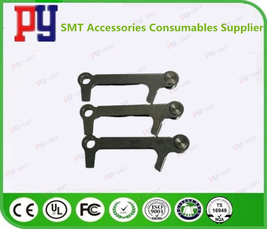
Overall Rating
Rating Snapshot
The following is the distribution of all ratingsAll Reviews